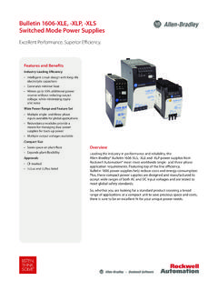
Transcription of Current Mode Control PWM Regulator IC For …
1 STR-A60xxHDescriptionThe STR-A60xxH series are power ICs for switching power supplies , incorporating a power MOSFET and a Current mode PWM controller IC. Including a startup circuit and a standby function in the controller, the product achieves low power consumption, low standby power , and high cost-effectiveness power supply systems with few external STR-A60xxH internal MOSFET has a VDSS of 650 V(min) or 700 V(min), and an RDS(on) of or with a frequency of 100 kHz. power output is rated at 10 or 15 W at 230 VAC input and 8 or 13 W at wide input range (85 to 265 VAC).
2 The device is provided in an industry-standard DIP-8 package, with pin 6 removed for increased isolation. Features and Benefits Small DIP8 package with10 to 15 W power output 230 VAC Current Mode PWM Control with 100 kHz switching frequency Built-in Random switching function, reducing EMI noise, and simplifying EMI filters, and therefore reducing cost Built-in Slope Compensation function, avoiding subharmonic oscillation Built-in Auto Standby function (Input power , PIN < 25 mW at no load) Normal operation: PWM mode Light load operation.
3 Standby mode (burst oscillation) Built-in Audible Noise Suppression function during Standby mode Built-in Startup Circuit, reducing power consumption in standby operation, and eliminating external components. Bias-Assist function, improving startup operation, suppressing VCC voltage drop in operation, and allowing use of smaller VCC capacitorCurrent Mode Control PWM Regulator IC For switching power SuppliesTypical ApplicationNot to scaleContinued on the next (AC)GNDOUTGNDFB/OLP7D/STApplications: for switching power supplies used in.
4 Battery chargers for cell phones, digital cameras, video cameras, shavers, emergency lights Stand-by power for LCD TVs, desktop PCs, LB Printers, audio equipment Small switched-mode power supplies for inkjet printers, DVD/CD players, set-top boxes Auxiliary power supplies for A/C, refrigerators, washers, dish washers, and other white goodsPackage: 8-pin DIPSTRA60xxH-DSCurrent Mode Control PWM Regulator IC For switching power SuppliesSTR-A60xxH2 Features and Benefits (continued) Built-in Leading Edge Blanking function Built-in High Speed Latch Release function, releasing the latch shutdown immediately at turning off AC supply Two-chip structure, with a controller and a power MOSFET with guaranteed avalanche energy available to simplify surge absorber circuits Protection functions: Brown-In and Brown-Out Protection function.
5 Auto-restart, prevention of excess input Current and heat rise at low input voltage Overcurrent Protection function (OCP): pulse-by-pulse built-in compensation circuit to minimize OCP point variation on AC input voltage Overload Protection function (OLP): auto-restart, built-in timer, reduces heat during overload condition, and no external components required Overvoltage Protection function (OVP): latched shutdown Thermal Shutdown Protection function (TSD): shutdown latches device off to prevent continuous oscillationSelection GuidePart NumberfOSC(kHz)MOSFETVDSS(min)(V)RDS(on) (max)( )POUT*(W)PackagePacking230 with pin 6 removed50 pieces per * The listed output power is based on the package thermal ratings, and the peak output power can be 120% to 140% of the value stated here.
6 At low output voltage and short duty cycle, the output power may be less than the value stated MicroSystems, Northeast CutoffWorcester, Massachusetts 01615-0036 ; Mode Control PWM Regulator IC For switching power SuppliesSTR-A60xxH3 Absolute Maximum Ratings1 Valid at TA = 25 C, unless otherwise specifiedCharacteristicSymbolNotesTermin alsRatingUnitDrain Current2 IDpeakSingle pulseSTR-A6059H8 Pulse Avalanche Energy3 EASS ingle pulse, VDD = 99 V, L = 20 mHSTR-A6059H8 124mJSTR-A6062H8 156mJSTR-A6069H8 124mJILpeakSingle pulse, VDD = 99 V, L = 20 mHSTR-A6059H8 Terminal VoltageVOCP1 3 2 to 6 VController IC (MIC)
7 Supply Input VoltageVCC5 332 VFB/OLP Terminal VoltageVFB4 3 to 14 VFB/OLP Terminal Sink CurrentIFB4 Terminal VoltageVBR2 3 to 7 VBR Terminal Sink CurrentIBR2 power Dissipation4PD1 Mounted on a 15 mm 15 mm PCB8 IC (MIC) power DissipationPD25 Ambient TemperatureTOPM aximum recommended internal leadframe temperature, TF(max) = 115 C 20 to 125 CStorage TemperatureTstg 40 to 125 CChannel TemperatureTch 150 C1 Current characteristics are defined based on IC as sink ( +), or source ( ). 2 Refer to MOSFET Safe Operating Area to MOSFET Avalanche Energy Derating Coefficient to MOSFET Temperature versus power Dissipation MicroSystems, Northeast CutoffWorcester, Massachusetts 01615-0036 ; Mode Control PWM Regulator IC For switching power SuppliesSTR-A60xxH4D/S TVCC524S/OCPFB/OLPGNDBRDRVPWM OSCREGSQRS lopeCo mp ensatio VVREGFe edbackControlOCPD rain Peak CurrentCompe nsa ti on7 V12.
8 8 VVCCLEBOLPO vervoltageProtection (OVP)ThermalShutdown (TSD)StartupUVLOB rown-In/Brown-Out7,813 Functional Block Diagram123487 5D/STD/STVCCS/OCPBRGNDFB/OLPPin-out DiagramTerminal List TableNumberNameFunction1S/OCPMOSFET source, and input for Overcurrent Protection detection signal2 BRInput for Brown-In and Brown-Out Protection detection voltage3 GNDG round4FB/OLPI nput for constant voltage Control signal, and input for Overload Protection signal5 VCCI nput for power supply for Control circuit6 (Pin removed)7, 8D/STMOSFET drain, and input for startup currentAllegro MicroSystems, Northeast CutoffWorcester, Massachusetts 01615-0036.
9 Mode Control PWM Regulator IC For switching power SuppliesSTR-A60xxH5 Electrical Characteristics1 Valid at VCC = 18 V, TA = 25 C, unless otherwise Start VoltageVCC(ON)5 Stop Voltage2 VCC(OFF)5 Current in OperationICC(ON)5 3 Startup VoltageVST(ON)5 3 38 VStartup CurrentISTARTUP5 3 Current Supply Threshold Voltage2 VCC(BIAS)5 switching FrequencyfOSC(av)8 390100110kHzSwitching Frequency Variance Range f8 3 8 kHzMaximum Duty CycleDMAX8 3778389%Minimum On-TimetON(MIN) 470 nsLeading Edge Blanking TimetBW 280 nsOCP Compensation CoefficientDPC 33 mV/ sMaximum Duty Cycle for OCP CompensationDDPC 36 %OCP Threshold Voltage at Zero Duty CycleVOCP(L)1 Threshold Voltage at 36% Duty CycleVOCP(H)1 Feedback CurrentIFB(MAX)4 3 340 230 150 AMinimum Feedback CurrentIFB(MIN)4 3 30 15 7 AOscillation Stop FB/OLP VoltageVFB(OFF)4 Threshold VoltageVFB(OLP)4 Delay TimetOLP4 3546882msOperation Current After OLPICC(OLP)5 3 300600 AFB/OLP Terminal Clamp VoltageVFB(CLAMP)
10 4 Threshold VoltageVBR(IN)2 Threshold VoltageVBR(OUT)2 Terminal Clamp VoltageVBR(CLAMP)2 Function Disabling ThresholdVBR(DIS)2 Threshold VoltageVCC(OVP)5 3262932 VLatch Circuits Sustaining Current3 ICC(LATCH)5 3 700 AThermal Shutdown Operating TemperatureTJ(TSD)5 3135 C1 Current characteristics are defined based on IC as sink ( +), or source ( ). 2 VCC(BIAS) > VCC(OFF). 3A latch circuit is a circuit operated with Overvoltage Protection (OVP) and/or Thermal Shutdown Protection (TSD) in MicroSystems, Northeast CutoffWorcester, Massachusetts 01615-0036.