Transcription of Datasheet REV1.2 UNIVERSAL ISM BAND FSK TRANSCEIVER …
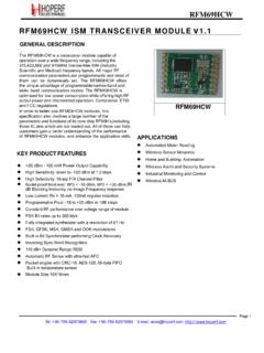
1 RFM12B Datasheet UNIVERSAL ISM band FSK TRANSCEIVER MODULE RFM12B RFM12B the purpose of this spec covers mainly for the physical characteristic of the module, for register configure and its related command info please refer to RF12B data sheets General Introduction RFM12B is a low costing ISM band TRANSCEIVER module implemented with unique PLL. It works signal ranges from 433/868/915 MHZ bands, comply with FCC, ETSI regulation. The SPI interface is used to communicate with microcontroller for parameter setting. Features: Low costing, high performance and price ratio Tuning free during production PLL and zero IF technology Fast PLL lock time High resolution PLL with KHz step High data rate (up to kbps with internal demodulator with external RC filter highest data rate is 256 kbps) Differential antenna input/output Automatic antenna tuning Programmable TX frequency deviation (from 15 to 240 KHz) Programmable receiver bandwidth (from 67 to 400 kHz) Analog and digital signal strength indicator (ARSSI/DRSSI) Automatic frequency control (AFC) Data quality detection (DQD)
2 Internal data filtering and clock recovery RX synchron pattern recognition SPI compatible serial control interface Clock and reset signal output for external MCU use 16 bit RX Data FIFO Two 8 bit TX data registers Standard 10 MHz crystal reference Wakeup timer power supply Low power consumption Standby current less than Supports very short packets (down to 3 bytes) Tel: +86-755-82973805 Fax: +86-755-82973550 E-mail: RFM12B Datasheet Typical Application Remote control Remote sensor Wireless data collection Home security system Toys Tire pressure monitoring system Pin Definition SMD DIP definition Type Function nINT/VDI DI/ DO Interrupt input (active low)/Valid data indicator VDD S Positive power supply SDI DI SPI data input SCK DI SPI clock input nSEL DI Chip select (active low) SDO DO Serial data output with bus hold nIRQ DO Interrupts request output active low FSK/DATA/nFFS DI/DO/DI Transmit FSK data input/ Received data output (FIFO not used)/ FIFO select DCLK/CFIL/FFIT DO/AIO/DO Clock output (no FIFO )/ external filter capacitor(analog mode)
3 / FIFO interrupts(active high)when FIFO level set to 1, FIFO empty interruption can be achieved CLK DO Clock output for external microcontroller nRES DIO Reset output active low GND S Power ground Electrical Parameter Maximum not at working mode symbol parameter minimum maximum Unit VddPositive power supply V VinAll pin input level Vdd+ V Tel: +86-755-82973805 Fax: +86-755-82973550 E-mail: RFM12B Datasheet Tel: +86-755-82973805 Fax: +86-755-82973550 E-mail: IinInput current except power -25 25 mA ESD Human body model 1000 V TstStorage temperature -55 125 C TldSoldering temperature(10s) 260 C Recommended working range symbol parameter minimum maximum Unit VddPositive power supply V TopWorking temperature -40 85 C DC characteristic symbol parameter Remark minimumtypical maximum UnitIdd_TX_0 Supply current (TX mode, Pout = 0dBm) 315,433 MHz band 868 MHz band 915 MHz band 15 16 17 17 18 19 mA Idd_TX_PMAXS upply current (TX mode, Pout = Pmax) 315,433 MHz band 868 MHz band 915 MHz band 22 23 24 24 25 26 mA Idd_RXSupply current (RX mode)
4 315,433 MHz band 868 MHz band 915 MHz band 11 12 13 13 14 15 mA IxIdle current Crystal oscillator on mA IpdSleep mode current All blocks off uA IlbLow battery detection uA VlbLow battery detect threshold per step V VlbaLow battery detection accuracy 0 5 % VilLow level input *VddV VihHigh level input *Vdd V IilLeakage current Vil=0V -1 1 uA IihLeakage current Vih=Vdd, Vdd= -1 1 uA VolLow level output Iol=2mA V VohHigh level output Ioh=-2mA V AC characteristic symbol parameter remark min typical max Unit frefPLL frequency 9 10 11 MHz fLO frequency (10 MHz crystal used) 433 MHz band , step 868 MHz band ,5 KHz step 915 MHz band , step MHz RFM12B Datasheet Tel: +86-755-82973805 Fax: +86-755-82973550 E-mail.
5 FLO frequency (9 MHZ crystal used) 433 MHz band , step 868 MHz band ,5 KHz step 915 MHz band , step MHz fLO frequency (11 MHZ crystal used) 433 MHz band , step 868 MHz band ,5 KHz step 915 MHz band , step MHz BW Receiver bandwidth mode 0 mode 1 mode 2 mode 3 mode 4 mode 5 60 120 180 240 300 360 67 134 200 270 350 400 75 150 225 300 375 450 KHz tlockPLL lock time After 10 MHz step hopping, frequency error <10 kHz 30 us tst, P PLL startup time With a running crystal oscillator 200 300 us BR Data rate With internal digital demodulator BRAData rate With external RC filter 256 kbps BER 10-3, BW=134 KHz,BR= , 433 MHz band -109 -100 BER 10-3, BW=134 KHz,BR= , 868 MHz band -105 -100 Pmin sensitivity BER 10-3, BW=134 KHz,BR=.
6 915 MHz band -105 -100 dBm AFCrangeAFC working range dfFSK : FSK deviation in the received signal * dfFSK RSARSSI accuracy 5 dB RSRRSSI range 46 dB CARSSIARSSI filter 1 nF RSSTEPRSSI programmable step 6 dB RSRESPDRSSI response time RSSI output high after valid , CARRSI=5nF 500 us RFM12B Datasheet Tel: +86-755-82973805 Fax: +86-755-82973550 E-mail: AC characteristic(Transmitter) symbol parameter remark min typical max Unit 433 MHz band 3 5 868 MHz band 2 4 Pmax Max.
7 Available output power 915 MHz band 2 4 dBm PoutTypical output power Selectable in 3 dB steps Pmax-21 Pmaxdbm CoOutput capacitance (set by the automatic antenna tuning circuit) In low bands In high bands 2 pf QoQuality factor of the output capacitance In low bands In high bands 13 8 15 10 17 12 LoutOutput phase noise 100 kHz from carrier 1 MHz from carrier -80 -103 dbc/HZ BRTXFSK bit rate Via internal TX data register 172 kbps BRATXFSK bit rate TX data connected to the FSK input 256 kbps dffskFSK frequency deviation Programmable in 15 kHz steps 15 240 kHZ AC characteristic(Turn-on/Turnaround timings) symbol parameter remark mintypical max UnitTstCrystal oscillator startup time Crystal ESR < 100 1 5 ms Ttx_XTAL_ONTransmitter turn-on time Synthesizer off, crystal oscillator on with 10 MHz step 250 us Trx_XTAL_ONReceiver turn-on time Synthesizer off, crystal oscillator on with 10 MHz step 250 us Ttx_rx_SYNT_ONTransmitter Receiver turnover time Synthesizer and crystal oscillator on during TX/RX change with 10 MHz step 150 us Trx_tx_SYNT_ONReceiver Transmitter turnover time Synthesizer and crystal oscillator on during RX/TX change with 10 MHz step 150 us CxlCrystal load capacitance Programmable in pF steps.
8 Tolerance+/- 10% 16 pf tPORI nternal POR timeout After Vdd has reached 90% of final value 100 ms tPBtWake-up timer clock period Calibrated every 30 seconds ms Cin, DDigital input apacitance 2 pf tr, fDigital output rise/fall time 15pF pure capacitive load 10 ns RFM12B Datasheet Field testing range band Test condition Distance 433 MHz band Receiver bandwidth =67 KHz, data rate= , transmitter frequency deviation =45 KHZ matches with RFM12 In free open area >200M 868 MHz band Receiver bandwidth=67 KHz,data rate = ,Transmitter frequency deviation =45 KHZ matches with RFM12 in free open area >200M 915 MHz band Receiver bandwidth=67 KHz,data rate = ,Transmitter frequency deviation =45 KHZ matches with RFM12 in free open area >200M SGS Reports Tel: +86-755-82973805 Fax: +86-755-82973550 E-mail: RFM12B Datasheet Tel: +86-755-82973805 Fax: +86-755-82973550 E-mail: RFM12B Datasheet Mechanical Dimension units in mm SMD PACKAGE S1 SMD PACKAGE S2 Tel: +86-755-82973805 Fax: +86-755-82973550 E-mail: RFM12B Datasheet DIP PACKAGE D Tel: +86-755-82973805 Fax: +86-755-82973550 E-mail: RFM12B Datasheet Module Model Definition model=module-operation_band-package_type RFM12B 433-DTel: +86-755-82973805 Fax: +86-755-82973550 E-mail: module type operation band Package example 1 RFM12B module at 433 MHz band , DIP : RFM12B-433-D 2 RFM12B module at 868 MHZ band , SMD, thickness at : RFM12B-868-S1 HOPE MICROELECTRONICS CO.
9 ,LTD Add:4/F, Block B3, East Industrial Area, Huaqiaocheng, Shenzhen, Guangdong, China Tel: 86-755-82973805 Fax: 86-755-82973550 Email: Website: This document may contain preliminary information and is subject to change by Hope Microelectronics without notice. Hope Microelectronics assumes no responsibility or liability for any use of the information contained herein. Nothing in this document shall operate as an express or implied license or indemnity under the intellectual property rights of Hope Microelectronics or third parties. The products described in this document are not intended for use in implantation or other direct life support applications where malfunction may result in the direct physical harm or injury to persons. NO WARRANTIES OF ANY KIND, INCLUDING, BUT NOT LIMITED TO, THE IMPLIED WARRANTIES OF MECHANTABILITY OR FITNESS FOR A ARTICULAR PURPOSE, ARE OFFERED IN THIS DOCUMENT. 2006, HOPE MICROELECTRONICS CO.
10 ,LTD. All rights reserved.