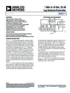
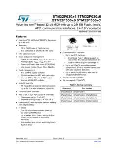
Transcription of Datasheet - STM8S001J3 - 16 MHz STM8S 8-bit MCU, 8-Kbyte ...
1 This is information on a product in full production. August 2020DS12129 Rev 41/84 STM8S001J316 MHz STM8S 8-bit MCU, 8-Kbyte Flash memory, 128-byte data EEPROM, 10-bit ADC, 3 timers, UART, SPI, I2 CDatasheet - production dataFeaturesCore 16 MHz advanced STM8 core with Harvard architecture and 3-stage pipeline Extended instruction setMemories Program memory: 8-Kbyte Flash memory; data retention 20 years at 55 C after 100 cycles RAM: 1 Kbyte Data memory: 128-byte true data EEPROM; endurance up to 100 k write/erase cyclesClock, reset and supply management V to V operating voltage Flexible clock control, 3 master clock sources External clock input Internal, user-trimmable 16 MHz RC Internal low-power 128 kHz RC Clock security system with clock monitor Power management Low-power modes (wait, active-halt, halt) Switch-off peripheral clocks individually Permanently active, low-consumption power-on and power-down resetInterrupt management Nested interrupt controller with 32 interrupts Up to 5 external interruptsTimers Advanced control timer.
2 16-bit, 2 CAPCOM channels, 2 outputs, dead-time insertion and flexible synchronization 16-bit general purpose timer, with 3 CAPCOM channels (IC, OC or PWM) 8-bit basic timer with 8-bit prescaler Auto wakeup timer Window and independent watchdog timersCommunications interfaces UART, SmartCard, IrDA, LIN master mode SPI unidirectional interface up to 8 Mbit/s (master simplex mode, slave receiver only) I2C interface up to 400 Kbit/sAnalog to digital converter (ADC) 10-bit ADC, 1 LSB ADC with up to 3 multiplexed channels, scan mode and analog watchdog Internal reference voltage measurementI/Os Up to 5 I/Os including 4 high-sink outputs Highly robust I/O design, immune against current injectionDevelopment support Embedded single-wire interface module (SWIM) or fast on-chip programming and non-intrusive mm or 150 mils Rev 4 Contents1 Introduction.
3 82 Description .. 93 Block diagram .. 104 Functional overview .. processing unit STM8 .. wire interface module (SWIM) and debug module (DM) .. controller .. program memory and data EEPROM .. controller .. management .. timers .. wakeup counter .. - 16-bit advanced control timer .. - 16-bit general purpose timer .. - 8-bit basic timer .. converter (ADC1) .. interfaces .. 205 Pinouts and pin descriptions .. SO8N pinout and pin description .. function remapping .. 246 Memory and register map .. map .. map .. port hardware register map .. hardware register map .. 28DS12129 Rev 43 module/interrupt controller registers.
4 347 Interrupt vector mapping .. 368 Option bytes .. function remapping bits .. 399 Electrical characteristics .. conditions .. and maximum values .. values .. curves .. capacitor .. input voltage .. maximum ratings .. conditions .. external capacitor .. current characteristics .. clock sources and timing characteristics .. clock sources and timing characteristics .. characteristics .. port pin characteristics .. serial peripheral interface .. interface characteristics .. ADC characteristics .. characteristics .. 7210 Package information .. package information .. characteristics .. document.
5 The product temperature range .. 7811 Ordering information .. 8012 STM8 development tools .. and in-circuit debugging tools .. 81 ContentsSTM8S001J34/84DS12129 Rev tools .. toolset .. and assembly toolchains .. tools .. 8213 Revision history .. 83DS12129 Rev 45/84 STM8S001J3 List of tables6 List of tablesTable features .. 9 Table clock gating bit assignments in CLK_PCKENR1/2 registers .. 15 Table timer features.. 18 Table for STM8S001J3 pin description tables.. 21 Table pin description .. 22 Table , Data EEPROM and RAM boundary addresses .. 26 Table port hardware register map .. 26 Table hardware register map .. 28 Table module/interrupt controller registers.
6 34 Table mapping .. 36 Table bytes .. 37 Table byte description .. 37 Table alternate function remapping bits for 8-pin devices .. 39 Table characteristics .. 41 Table characteristics .. 42 Table characteristics.. 42 Table operating conditions .. 43 Table conditions at power-up/power-down .. 44 Table current consumption with code execution in run mode at VDD = 5 V .. 45 Table current consumption with code execution in run mode at VDD = V .. 45 Table current consumption in wait mode at VDD = 5 V .. 46 Table current consumption in wait mode at VDD = V .. 46 Table current consumption in active halt mode at VDD = 5 V .. 47 Table current consumption in active halt mode at VDD = V.
7 47 Table current consumption in halt mode at VDD = 5 V .. 48 Table current consumption in halt mode at VDD = V .. 48 Table times .. 48 Table current consumption and timing in forced reset state .. 49 Table current consumption .. 49 Table user external clock characteristics .. 53 Table oscillator characteristics.. 54 Table oscillator characteristics .. 54 Table and hardware registers .. 56 Table program memory and data EEPROM .. 56 Table static characteristics .. 57 Table driving current (standard ports) .. 59 Table driving current (true open drain ports).. 59 Table driving current (high sink ports).. 60 Table characteristics .. 65 Table characteristics.
8 67 Table characteristics .. 69 Table accuracy with RAIN < 10 k , VDD = 5 V.. 70 Table accuracy with RAIN < 10 k RAIN, VDD = V .. 70 Table data .. 72 Table data .. 73 Table absolute maximum ratings .. 73 Table sensitivities .. 74 Table 8-lead x 6 mm, plastic small outline, 150 mils body width, List of tablesSTM8S001J36/84DS12129 Rev 4package mechanical data .. 75 Table characteristics.. 78 Table revision history .. 83DS12129 Rev 47/84 STM8S001J3 List of figures7 List of figuresFigure block diagram .. 10 Figure memory organization .. 13 Figure SO8N pinout .. 21 Figure map .. 25 Figure loading conditions .. 40 Figure input voltage.
9 41 Figure versus VDD .. 43 Figure capacitor CEXT .. 44 Figure IDD(RUN) vs VDD, HSE user external clock, fCPU = 16 MHz .. 50 Figure IDD(RUN) vs fCPU, HSE user external clock, VDD = 5 V .. 50 Figure IDD(RUN) vs VDD, HSI RC osc, fCPU = 16 MHz .. 51 Figure IDD(WFI) vs. VDD HSE user external clock, fCPU = 16 MHz .. 51 Figure IDD(WFI) vs. fCPU, HSE user external clock, VDD = 5 V .. 52 Figure IDD(WFI) vs VDD, HSI RC osc, fCPU = 16 MHz .. 52 Figure external clock source .. 53 Figure LSI frequency variation vs VDD @ 4 temperatures .. 55 Figure VIL and VIH vs VDD @ 4 temperatures .. 58 Figure pull-up resistance vs VDD @ 4 temperatures .. 58 Figure pull-up current vs VDD @ 4 temperatures.
10 59 Figure VOL @ VDD = 5 V (standard ports) .. 60 Figure VOL @ VDD = V (standard ports) .. 61 Figure VOL @ VDD = 5 V (true open drain ports) .. 61 Figure VOL @ VDD = V (true open drain ports) .. 62 Figure VOL @ VDD = 5 V (high sink ports) .. 62 Figure VOL @ VDD = V (high sink ports) .. 63 Figure VDD - VOH @ VDD = 5 V (standard ports) .. 63 Figure VDD - VOH @ VDD = V (standard ports) .. 64 Figure VDD - VOH @ VDD = 5 V (high sink ports) .. 64 Figure VDD - VOH @ VDD = V (high sink ports) .. 65 Figure timing diagram - slave mode and CPHA = 0 .. 66 Figure timing diagram - slave mode and CPHA = 1(1) .. 66 Figure timing diagram - master mode.