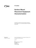
Transcription of Date IPC-SM-782 Surface Mount Design and Land …
1 INTRODUCTIONThis section covers land patterns for various discrete compo-nents. Each subsection contains information in accordancewith the following Component Description (Figure 1) Dimensions (Figure 2) Pattern Dimensions (Figure 3) and Solder Joint Analysis (Figure 4)The following is the table of contents for this section:Table of ContentsRectangular Leadless CapacitorsCircular Leadless (Metal Electrode Face) Resistors and DiodesSmall Outline Transistors (SOT) and Diodes (SOD) 223 Modified Through-Hole (TO) Packsfor Transistors and APPLICABLE DOCUMENTSThe following documents, of the issue in effect on the revisiondate of this section, form a part of this specification to theextent specified Electronic Industries Association (EIA)
2 1 EIA-PDP-100 Registered and Standard Mechanical Outlinesfor Electronic PartsEIA-481-ATaping of Surface Mount Components for Auto-matic PlacementEIA-481-18 mm and 2 mm Taping of Surface Mount Com-ponents for Automatic HandlingEIA-481-216 mm and 24 mm Embossed Carrier Taping ofSurface Mount Components for Automated HandlingEIA-481-332 mm, 44 mm, and 56 mm Embossed CarrierTaping of Surface Mount Components for Automated International Electrotechnical Commission (IEC)2 IEC 97 Grid System for Printed GENERAL PackagingDiscrete components are generally pur-chased in 8 mm and 12 mm wide tape and reel.
3 See Figure1. EIA-481 is the applicable specification for tape and your manufacturers guide for the packaging availabil-ity of your susceptible to damage by electrostatic discharge shallbe supplied in a manner that prevents such damage. Tapepeel strength shall be 40 30 grams. Peel from the top for thetop cover of the tape. Reel materials used in the constructionof the reel shall be easily disposable metal, chip board, sty-rene plastic or equivalent. Reels shall not cause deteriorationof the components or their solderability. Reels must be able towithstand high humidity 1 PackagingTop cover tapeSprocket holeComponent cavity Embossed carrier tapeSprocket holeEmbossed carrier tapeComponent cavity tttttttIPC-SM-782 Surface Mount Designand Land Pattern StandardDate8 Resistance to Cleaning ProcessesParts must becapable of withstanding cleaning processes currently used byboard assembly manufacturers.
4 This may include as a mini-mum 4-minute exposures to solvent cleaning solutions at40 C, plus a minimum of a 1-minute exposure to ultrasonicimmersion at a frequency of 40 kHz and a power of 100 wattsper square foot. Alkaline systems in use shall also not damageparts or remove Application for copies should be addressed to EIA, 2001 Pennsylvania Ave , Washington, DC, 20006-1813 orGlobal Engineering Documents, 1990 M St. , Wash-ington, DC Application for copies should be addressed to IEC, 3 ruede Varembe, PO Box 131 1211 Geneva 20, SwitzerlandIPC-SM-782 SubjectDiscrete ComponentsDate8 SCOPEM icrominiature leadless devices are available to the circuitdesigner in rectangular form for discrete components such aschip subsection provides the component and land patterndimensions for chip resistors, along with an analysis of toler-ance and solder joint assumptions used to arrive at the landpattern dimensions.
5 Basic construction of the chip resistor isalso APPLICABLE DOCUMENTSSee Section for documents applicable to the COMPONENT DESCRIPTIONSA variety of values exist for resistors. The following sectionsdescribe the most common Basic ConstructionThe resistive material is applied toa ceramic substrate and terminated symmetrically at bothends with a wrap around metal U-shaped band. The resis-tive material is face-up, thus trimming to close tolerances ispossible. Since most equipment uses a vacuum-type pickuphead, it is important that the Surface of the resistor is made flatafter trimming, otherwise vacuum pickup might be Figure Termination MaterialsEnd terminations should besolder coated with a tin/lead alloy.
6 The solder should containbetween 58 to 68% tin. Solder may be applied to the termi-nation by hot dipping or by plating from solution. Plated sol-der terminations should be subjected to a post-plating reflowoperation to fuse the solder. The tin/lead finish should be atleast mm [ in.] termination shall be symmetrical, and shall not have nod-ules lumps, protrusions, etc., that compromise the symmetryor dimensional tolerances of the part. The end terminationshall cover the ends of the components, and shall extend outto the top and bottom of the finish applied over precious metal electrodes shall havea diffusion-barrier layer between the electrode metalizationand the solder finish.
7 The barrier layer should be nickel or anequivalent diffusion barrier, and should be at least [ in] MarkingResistors equal to or larger than 2012[0805] are labeled. Resistors smaller than 1608 [0603] aregenerally Carrier Package FormatBulk rods, 8 mm tape/4mm pitch is preferred for best handling. Tape and reel speci-fications provide additional Resistance to SolderingParts should be capable ofwithstanding five cycles through a standard reflow systemoperating at 215 C. Each cycle shall consist of 60 secondsexposure at 215 C. Parts must also be capable of withstand-ing a minimum of 10 seconds immersion in molten solder at260 1 Chip resistor constructionResistorAlumina ChipPlatinum-silverWrap-aroundterminatio nWire Bond ConstructionGlassPassivationIPC-SM-782 Surface Mount Designand Land Pattern StandardDate5 COMPONENT DIMENSIONSF igure 2 provides the component dimensions for [in]ComponentIdentifierLSWTH minmaxminmaxminmaxminmaxmax1005 [0402] [0603] [0805] [1206] [1210] [2010] [2512]
8 2 Chip resistor component dimensions LSTWHIPC-782-8-1-2 IPC-SM-782 SubjectChip ResistorsDate5 LAND PATTERN DIMENSIONSF igure 3 provides the land pattern dimensions for chip resis-tors. These numbers represent industry consensus on thebest dimensions based on empirical knowledge of fabricatedland the table, the dimensions shown are at maximum materialcondition (MMC). The least material condition (LMC) shouldnot exceed the fabrication (F) allowance shown on page LMC and the MMC provide the limits for each dotted line in Figure 3 shows the grid placement court-yard which is the area required to place land patterns andtheir respective components in adjacent proximity withoutinterference or shorting.
9 Numbers in the table represent thenumber of grid elements (each element is by mm) inaccordance with the international grid detailed in IEC publica-tion Identifier(mm) [in.]Z (mm)G (mm)X (mm)Y (mm)C (mm)Placement Grid(No. of Grid Elements)refref100A1005 [0402] [0603] [0805]* [1206]* [1210]* [2010]* [2512]* *Note:If a more robust pattern is desired for wave soldering devices larger than 1608 [0603], add mm to theY-dimension, and consider reducing the X-dimension by 30%. Add a W suffix to the number; , 3 Chip resistor land pattern dimensionstttttttttCGZXYG ridplacementcourtyardtIPC-782-8-1-3 IPC-SM-782 SubjectChip ResistorsDate5 TOLERANCE AND SOLDER JOINT ANALYSISF igure 4 provides an analysis of tolerance assumptions andresultant solder joints based on the land pattern dimensionsshown in Figure 3.
10 Tolerances for the component dimensions,the land pattern dimensions (fabrication tolerances on theinterconnecting substrate), and the component placementequipment accuracy are all taken into 4 provides the solder joint minimums for toe, heel, andside fillets, as discussed in Section The tolerances areaddressed in a statistical mode, and assume even distributionof the tolerances for component, fabrication, and tolerances for fabrication ( F ) and componentplacement equipment accuracy ( P ) are assumed, and aregiven in the table. These numbers may be modified based onuser equipment capability or fabrication criteria.