Transcription of DC TO DC CONVERTER CONTROLLER
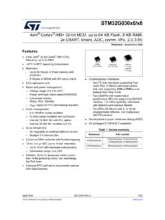
1 DC TO DC CONVERTER CONTROLLER DESCRIPTION The MC34063 is a monolithic regulator subsystem, intended for use as DC to DC CONVERTER . This device contains a temperature compensated band gap reference, a duty-cycle control oscillator, driver and high current output switch. It can be used for step down, step-up or inverting switching regulators as well as for series pass regulators. FEATURES * Operation from to 40V. * Short circuit current limiting. * Low standby current. * Output switch current of without external transistors. * Frequency of operation from 100Hz to 100kHz. * Step-up, step-down or inverting switch regulators. PIN CONFIGURATION PIN DESCRIPTION PIN NO PIN NAME I/O DESCRIPTION 1 Switch Collector I Internal Darlington pairs TI collector 2 Switch Emitter O Internal Darlington pairs TI emitter 3 Timing Capacitor The value of selected capacitor controls the internal oscillator run rate 4 GND 5 Comparator Inverting Input I Inverting input of comparator which can set & initiate the Darlington pairs output switch 6 VCC 7 IPEAK Sense I Current sense input to monitor the voltage drop across an external resistor placed in series with VCC 8 Driver Collector I Internal Darlington pairs TI collector DIP-8MC34063S SOP-8 BLOCK DIAGRAM 87542136 QSRCET1T2 AIsDBCTVccGNDT iming CapacitorSwitch EmitterSwitch
2 InvertingInputIPEAK SenseDrive Collector ABSOLUTE MAXIMUM RATINGS (Ta=25 C ) PARAMETER SYMBOLRATINGS UNIT Supply Voltage VCC 40 V Comparator Input Voltage Range VIN(COMP) ~ +40 V Switch Collector Voltage VC(SW)40 V Switch Emitter Voltage VE(SW)40 V Switch Collector to Emitter Voltage VCE(SW)40 V Driver Collector Voltage VC(DR) 40 V Switch Current ISW A DIP-8 1250 Power Dissipation (Ta=25 C) SOP-8PD 625 mW Junction Temperature TJ +150 C Operating Temperature TOPR 0 ~ +70 C Storage Temperature TSTG -65 ~ +150 C Note: Absolute maximum ratings are those values beyond which the device which the device could be permanently damaged.
3 Absolute maximum ratings are stress ratings only and functional device operation is not implied. THERMAL DATA PARAMETER SYMBOLRATINGS UNIT DIP-8100 Junction-to-Ambient SOP-8 JA 160 C/W ELECTRICAL CHARACTERISTICS (VCC= , Ta=0~+70 C, unless otherwise specified.) PARAMETER SYMBOLTEST CONDITIONS MIN TYP MAX UNITO scillator Charging Current ICHG VCC=5 to 40V, Ta=25 C 22 31 42 ADischarging Current IDISCHG VCC=5 to 40V, Ta=25 C 140 190 260 AOscillator Amplitude VOSC Ta=25 C V Discharge to Charge Current Ratio K V7=VCC.
4 Ta=25 C Current limit Sense Voltage VSENSE ICHG=IDISCHG, Ta=25 C 250 300 350mVOutput Switch Saturation Voltage 1(Note) VCE(SAT)1 ISW= , VC(DRIVER)=VC(SW) Saturation Voltage 2(Note) VCE(SAT)2 ISW= , VC(DRIVER)=50mA DC Current Gain(Note) GI (DC) ISW= , VCE= , Ta=25 C 50 180 Collector Off State Current(Note) IC(OFF) VCE= , Ta=25 C 100 AComparator Threshold Voltage VTHD Threshold Voltage Line Regulation VTHD VCC=3 ~ 40V Bias Current II(BIAS) VIN=0V 50 400nATotal Device Supply Current ICC VCC=5~40V, CT= V7=VCC, VC>VTHD, Pin2=GND : Output switch tests are performed under pulsed conditions to minimize power dissipation.
5 170 H1N58191808L1234CT765 RSC REF ++ +VOUT28V/175mA100+ HOptional Filter STEP-UP CONVERTER (Cont.) STEP-DOWN CONVERTER (Cont.) VOLTAGE INVERTING CONVERTER DESIGN FORMULA TABLE CALCULATION STEP-DOWN STEP-UP VOLTAGE-INVERTING tONtOFF VOUT + VF VIN-VCE(SAT) (tON+tOFF)MAX CT 4x10⁻⁵ tON 4x10⁻⁵ tON 4x10⁻⁵ tON ISW 2 IOUT(MAX) RS L(MIN) CO IOUT tONVRIPPLE(P-P) VCE(SAT) - Saturation voltage of the output switch. VF - Forward voltage drop of the ringback rectifier. The following power supply characteristics must be chosen: VIN - Nominal input voltage.
6 VOUT - Desired output voltage, VOUT = (1+R2/R1) IOUT - Desired output current. FMIN - Minimum desired output switching frequency at the selected values for VIN and IOUT. VRIPPLE(P-P) - Desired peak-to-peak output ripple voltage. In practice, the calculated value will need to be increased due to the capacitor equivalent series resistance and board layout. The ripple voltage should be kept to a low value since it will directly effect the line and load regulation. TYPICAL CHARACTERISTICS