Transcription of DEMO ONLY Version - IPC
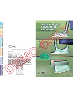
1 PhotosChip ComponentsJ-Lead ComponentsGull Wing ComponentsClass 3 Class 2 Class 1 IPC 2010 3000 Lakeside Drive, Suite 309-S Bannockburn, IL 60015-1219 +1 (tel.) +1 (fax) email: rights reserved under both international and Pan-American copyright conventions. Any copying, scanning or other reproduc-tions of these materials without the prior written consent of the copyright holder is strictly prohibited and constitutes infringement under the Copyright Law of the United Rev. E 3m Rev. D 4m Rev. D 5m Rev. C 3m Rev. B 3m Rev. A 5m 1st printing 5m Association Connecting Electronics IndustriesDEMO only VersionThis is a promotional sample of the IPC Training and Reference Guide do not use this SAMPLE for training or reference is a not-for-profit association for the electronics industry. Please respect our may order printed copies from IPC at: or call (847) you for viewing this DRM-SMT-E DRM-SMT-EChip ComponentsClass 1 Class 2J-Lead ComponentsGull Wing ComponentsClass 3 Photos1 TABLE OF CONTENTS Introduction 2 Acceptance Criteria 2 Lead Free 2 Classification 3 Terminology 4 Chip Components Class 1 Dimensional Criteria 6 Class 2 Dimensional Criteria 8 Class 3 Dimensional Criteria 10 Solder Conditions Photos 12 J-Lead Components Class 1 Dimensional Criteria 18 Class 2 Dimensional Criteria 20 Class 3 Dimensional Criteria 22 Solder Conditions Photos 24 Gull Wing Components Class 1 Dimensional Criteria 28 Class 2 Dimensional Criteria 30 Class 3 Dimensional Criteria 32 Solder Conditions Photos 34 Class 1 Class 2 Class 332 ClassificationSurface mount solder joint requirements are divided into three classes depending on the ultimate use.
2 Life expectancy and operating envi-ronment of the electronic assembly. These classes are as follows:Class 1 General Electronic ProductsConsumer type products, suitable for applications where the major requirement is how it functions, not necessarily for extended life, reli-ability of service, or cosmetic perfection. Class 2 Dedicated Service Electronic ProductsCommercial type products, where continued performance and extend-ed life is required and for which uninterrupted service is desired but not critical. Typically, the user environment is not extreme in such things as temperature or contamination, and would not cause failures. Class 3 High Performance Electronic Products Products where continued high performance or performance-on-demand is critical, equipment downtime cannot be tolerated, end-use environment may be uncommonly harsh, and the equipment must function when required, such as for life-support, flight control, and other high-reliability :The inspector does not select the class for the part under inspection.
3 Documentation which specifies the applicable class for the part under inspection should be provided to the Surface mount Solder Joint Evaluation Training and Reference Guide provides visual examples of conditions found in surface mount solder joints for three of the most popular termination styles: rectangular chip, J-lead and gull wing. It also defines the dimensional acceptability requirements for each, as determined by industry consensus standards This manual refer-ences and illustrates portions of the following two documents: First, the IPC-A-610 Rev. E, Acceptability of Electronic Assemblies, which illustrates the requirements for many types of solder connections. Second, the IPC J-STD-001 Rev. E, Requirements for Soldered Electronic Assemblies, which establishes the minimum acceptability CriteriaIn this Training and Reference Guide, minimum and maximum dimen-sional acceptance criteria are shown for each class of component type.
4 Solder joints falling outside these parameters will be deemed as unacceptable, according to the standards set in IPC-A-610 Rev. E and IPC J-STD-001 Rev. E. A target example is also given to show the ideal case scenario. Photographs of various solder conditions follow the dimensional cri-teria for each component :Accept and/or reject decisions must be based on applicable documentation, contract, drawings, referenced documents, and specifications such as the: IPC-A-610 and IPC J-STD-001. Denotes criteria that have changed from Revision D of these two Free Soldering The primary difference between the solder connections created with processes using tin-lead alloys and processes using lead free alloys is related to the visual appearance of the lead free and tin-lead connections may exhibit similar appearances, but lead free alloys are more likely to have:- Surface roughness (grainy or dull) - Greater wetting contact angles*All other solder criteria are the same.
5 *Wetting cannot always be judged by surface appearance. The wide range of solder alloys in use may exhibit from low or near zero degree contact angles to nearly 90 degree contact angles as Denotes Lead Free PhotosClass 3 Class 2 Class 1 Gull Wing ComponentsJ-Lead ComponentsChip ComponentsPhotosGull Wing ComponentsJ-Lead ComponentsChip Components54 TerminologyBelow are definitions that may be helpful in describing surface mount solder joints (also see: IPC-T-50):Adhesive In surface mounting, a glue used to adhere surface mount components to the printed wiring A number of components, subassemblies, or combinations thereof joined together on a printed wiring Hole A void in the solder joint caused by gas escaping from the molten The non-metallized, or non-leaded part of any electronic Rectangular Chip Component, a surface mounted electronic component with terminations, or metallized contact areas instead of leads.
6 Cold Solder Connection A solder connection that exhibits poor wetting and that is characterized by a gray, porous An individual part or combination of parts that, when together, perform an electrical Mounting The act of attaching components to the printed wiring board, or the method in which they are A single electrically conductive path in a larger conductive (Wetting) Angle The angle formed by the edge, or meniscus, of the solder fillet on the surface of the A condition failing to meet acceptability requirements, or is otherwise cause for A condition that results when molten solder coats a surface and then recedes to leave irregularly-shaped mounds of solder that are separated by an area that is covered with a thin film of solder, and with the basis metal not exposedDisturbed Solder Connection A solder connection that is characterized by an appearance caused by motion between the metals being joined while the solder was solidifying.
7 Excess Solder Connection A solder connection that is characterized by the complete obscuring of the surfaces of the connected metals and/or by the presence of solder beyond the connection A compound that, when heated, promotes the wetting of a base metal by molten Residue A flux-related contaminant that is present on or near the surface of a solder Wing A type of surface mount component lead that is bent in a configuration similar in shape to a seagull's The lowest bend in any surface mount lead, just before the lead makes actual contact with the A type of surface mount lead that is bent down and under the component, forming the shape of the letter J. Knee The uppermost bend of a component lead, closest to the component A portion of a conductive pattern that is usually used for making electrical connections, for component attachment, or A length of insulated or uninsulated metallic conductor that is used for electrical The partial adherence of molten solder to a surface that it has contacted and basis metal remains A small hole that penetrates from the surface of a solder connection to a void of indeterminate size within the solder Indicator A detectable variation in quality, other than a defect, that may be a reflection of improper material, equipment, personnel or Any visual or measurable form of process-related A metal alloy with a melting temperature that is below 427 C (800 F).
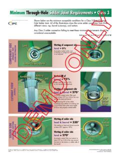
8 Solder Ball A small sphere of solder adhering to a laminate, resist, or conductor surface generally occurring after wave or reflow Bridging The unwanted formation of a conductive path of solder between Fillet A normally-concave surface of solder that is at the intersection of the metal surfaces of a solder Paste Finely divided particles of solder, with additives to promote wetting and other properties, suspended in a cream flux. The cream holds the surface mounted device in place until reflow The ability of a metal to be wetted by molten The joining of metallic surfaces with solder without the melting of the base Solder Condition An ideal solder connection, though not always achievable or necessary. One that is feathered-out to a thin edge, indicating proper solder flow and wetting action. With no sharp protrusions of solder or evidence of The metallized area of a chip component, the metallic lead of a component, or the land or terminal where a solder connection is The end or tip of a lead on a surface mount The complete lifting of a chip component, with one end having no solder connection to the A continuous film or curtain of solder that is parallel to, but not necessarily adhering to, a surface that should be free of The formation of a relatively uniform, smooth, unbroken film of solder to a basis ComponentsJ-Lead ComponentsGull Wing ComponentsClass 1 Class 2 Class 3 PhotosPhotosClass 3 Class 2 Class 1 Gull Wing ComponentsJ-Lead ComponentsChip ComponentsChip ComponentsClass 17 Chip ComponentsClass 16 End Joint Width (C)The width of the solder joint at its narrowest point must be a minimum of 50% the width of the component termination (W)
9 , or 50% of the width of the land (P), whichever is less. End Overlap (J)Some amount of overlap between the component termination and the land is required for minimum acceptance. Wetted solder fillet must also be Thickness (G)The minimum distance between the land and component termination is not specified. only a properly wetted fillet must be Height (F)Wetting is evident on termination s vertical surfaces as a minimum fillet height. Fillet Height (E)The solder may overhang the land, and extend onto the top of the termination, but not touch the top of the component body, as a maximum fillet Overhang (B)Any part of the component termination extending beyond the land is Overhang (A)The component may overhang the side of the land a maximum of 50% of the width of the component termination (W), or 50% of the width of the land (P), whichever is Components Class 1 This photo represents an ideal surface mount solder joint for any class of rectangular chip : Solder joints are semi-transparent to show relationship between land and termination.
10 Side Overhang, Dimension (A), must not violate minimum electrical clearance for assemblies with small devices. Minimum Side Joint Length, Dimension (D), is not required for chips, only a properly wetted fillet must be evident. The references below are applicable to the dimensional criteria for 1-, 3-, or 5-side termination Chip : A-610E: , Table 8-2; through J-STD-001E: , Table 7-4 Acceptance CriteriaAcceptance CriteriaPhotosClass 3 Class 2 Gull Wing ComponentsJ-Lead ComponentsClass 3 Class 2 Gull Wing ComponentsJ-Lead ComponentsTarget ConditionPhotosChip ComponentsClass 29 Chip ComponentsClass 28 This photo represents an ideal surface mount solder joint for any class of rectangular chip : Solder joints are semi-transparent to show relationship between land and termination. Side Overhang, Dimension (A), must not violate minimum electrical clearance for assemblies with small devices. Minimum Side Joint Length, Dimension (D), is not required for chips, only a properly wetted fillet must be evident.