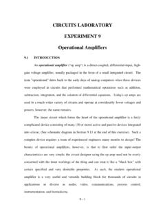
Transcription of Description Pin Assignments - Adafruit Industries
1 PAM8302A Document number: DSxxxxx Rev. 2 - 5 1 of 14 April 2013 Diodes Incorporated PAM8302AA Product Line ofDiodes FILTERLESS CLASS-D MONO AUDIO amplifier Description The PAM8302A is a Class-D mono audio amplifier . Its low THD+N feature offers high quality sound reproduction. The new filterless architecture allows the device to drive speakers directly instead of using low-pass output filters, therefore saving system cost and PCB area. With the same number of external components, the efficiency of the PAM8302A is much better than that of Class-AB cousins. It can optimize battery life thus is ideal for portable applications. The PAM8302A is available in MSOP-8, SOP-8, DFN3x3-8 and DFN2x2-8 packages.
2 Features Output at 10% THD with a 4 Load and 5V power Supply Filterless, Low Quiescent Current and Low EMI High Efficiency up to 88% Superior Low Noise Short Circuit Protection Thermal Shutdown, Few External Components to Save Space and Cost MSOP-8, SOP-8, DFN3x3-8 and DFN2x2-8 Packages Available Pb-Free Packages Applications PMP/MP4 GPS Portable Speakers Walkie Talkie Handsfree phones/Speaker Phones Cellular Phones Pin Assignments PAM8302A Document number: DSxxxxx Rev. 2 - 5 2 of 14 April 2013 Diodes Incorporated PAM8302AA Product Line ofDiodes Incorporated Typical Applications Circuit Functional Block Diagram Absolute Maximum Ratings (@TA = +25 C, unless otherwise specified.)
3 These are stress ratings only and functional operation is not implied. Exposure to absolute maximum ratings for prolonged time periods may affect device reliability. All voltages are with respect to ground. Parameter Rating Unit Supply voltage at No Input Signal V Input voltage to VDD + Maximum Junction Temperature 150 C Storage Temperature -65 to +150 Soldering Temperature 300, 5sec PAM8302A Document number: DSxxxxx Rev. 2 - 5 3 of 14 April 2013 Diodes Incorporated PAM8302AA Product Line ofDiodes Incorporated Recommended Operating Conditions (@TA = +25 C, unless otherwise specified.) Parameter Rating Unit Suppy voltage Range to V Operation Temperature Range -40 to +85 C Junction Temperature Range -40 to +125 C Thermal Information Parameter Package Symbol Max Unit Thermal Resistance (Junction to Ambient)
4 SOP-8 JA 115 C/W MSOP-8 180 DFN3x3-8 4739 DFN2x2-8 80 Electrical Characteristics (@TA = +25 C, VIN = , VO = , CIN = 10 F, COUT = 10 F, L = H, unless otherwise specified.) Parameter Symbol Test Conditions Min Typ Max Units Supply voltage Range VDD V Quiescent Current IQ No Load 4 8 mA Shutdown Current ISHDN VSHDN = 0V 1 A Output power PO f = 1kHz, RL = 4 , THD+N = 10% VDD = 5V W VDD = f = 1kHz, RL = 4.
5 THD+N = 1% VDD = 5V VDD = f = 1kHz, RL = 8 , THD+N = 10% VDD = 5V VDD = f = 1kHz, RL = 8 , THD+N = 1% VDD = 5V VDD = Peak Efficiency f = 1kHz 85 88 % Total Harmonic Distortion Plus Noise THD+N RL = 8 , PO = , f = 1kHz % RL = 8 , PO = , f = 1kHz RL = 4 , PO = , f = 1kHz RL = 4 , PO = , f = 1kHz Gain GV dB power Supply Ripple Rejection PSRR No Inputs, f = 1kHz, VPP = 200mV 45 50 dB Dynamic Range DYN f = 20 to 20kHz 85 90 dB Signal to Noise Ratio SNR f = 20 to 20kHz 75 80 dB Noise VN No A-Weighting 180 300 V A-Weighting 120 200 Oscillator Frequency fOSC 200 250 300 kHz Drain-Source On-State Resistance RDS(ON)
6 IDS = 100mA P MOSFET N MOSFET SHDN Input High VSH V SHDN Input Low VSL Over Temperature Protection OTP Junction Temperautre 120 135 C Over Temperature Hysterisis OTH 30 C PAM8302A Document number: DSxxxxx Rev. 2 - 5 4 of 14 April 2013 Diodes Incorporated PAM8302AA Product Line ofDiodes Incorporated Typical Performance Characteristics (@TA = +25 C, unless otherwise specified.) PAM8302A Document number: DSxxxxx Rev. 2 - 5 5 of 14 April 2013 Diodes Incorporated PAM8302AA Product Line ofDiodes Incorporated Typical Performance Characteristics (cont.)
7 (@TA = +25 C, unless otherwise specified.) PAM8302A Document number: DSxxxxx Rev. 2 - 5 6 of 14 April 2013 Diodes Incorporated PAM8302AA Product Line ofDiodes Incorporated Typical Performance Characteristics (cont.) (@TA = +25 C, unless otherwise specified.) PAM8302A Document number: DSxxxxx Rev. 2 - 5 7 of 14 April 2013 Diodes Incorporated PAM8302AA Product Line ofDiodes Incorporated Application Information Test Setup for Performance Testing PAM8302A DUT Notes: 1. The AP AUX-0025 low pass filter is necessary for every class-D amplifier measurement with AP analyzer. 2. Two 22 H inductors are used in series with load resistor to emulate the small speaker for efficiency measurement. Maximum Gain As shown in block diagram (Page 2), the PAM8302A has two internal amplifier stages.
8 The first stage's gain is externally con figurable, while the second stage's is internally fixed. The closedloop gain of the first stage is set by selecting the ratio of RF to RI while the second stage's gain is fixed at output of amplifier one serves as the input to amplifier two, thus the two amplifiers produce signals identical in magnitude, but different in phase by 180 . Consequently, the differential gain for the IC is A =20*log [2*(RF/RI)] The PAM8302A sets maximum R =80k , minimum RI =10k , so the maximum closed-gain is 24dB. Input Capacitor (CI) Intypical application, an input capacitor, CI is required to allow the amplifier to bias input signals to a proper DC level for optimum operation. In this case, CI and the minimum input impedance RI (10k internal) form a high pass filter with a corner frequeny determind by the following equation: CR21fIIC It is important to choose the value of CI as it directly affects low frequency performance of the circuit, for example, when an application requires a flat bass response as loas as 100Hz.
9 Equation is reconfigured as follows: fR21 CIII As the input reisitance is varible, for the CI value of F, one should actually choose the CI within the range of F to F. A further consideration for this capacitor is the leakage path from the input source through the input network (RI, RF, CI) to the load. This leakage current creates a DC offset voltage at the input to the amplifier that reduces useful headroom, especially in high gain application. For this reason, a low leakage tantalum or ceramic capacitor is the best choice. When a polarized capacitior is used, the positive side of the capacitor should face the amplifier input in most applications as the DC level is held at VDD/2, which is likely higher than the source DC level.
10 Please note that it is important to confirm the capacitor polarity in the application. PAM8302A Document number: DSxxxxx Rev. 2 - 5 8 of 14 April 2013 Diodes Incorporated PAM8302AA Product Line ofDiodes Incorporated Application Information (cont.) power Supply Decoupling (CS) The PAM8302A is a high-performance CMOS audio amplifier that requires adequate power supply decoupling to ensure the output THD and PSRR as low as possible. power supply decoupling affects low frequency response. Optimum decoupling is achieved by using two capacitors of different types that target different types of noise on the power supply leads. For higher frequency transients, spikes, or digital hash on the line, a good low equivalent-series-resistance (ESR) ceramic capacitor, typicall F is good, placing it as close as possilbe to the device VDD terminal.