Transcription of Design and Implementation of Open-Source SATA …
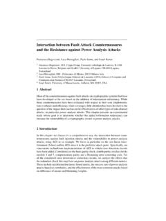
1 Design and Implementation of open -SourceSATA III Core for Stratix V FPGAsSumedh Guha1, Wen Wang1, Shafeeq Ibraheem1, Mahesh Balakrishnan2, and Jakub Szefer11 Dept. of Electrical Engineering and2 Dept. of Computer ScienceYale University{ , , , , sata is the de-facto standard computer interfacethat connects a host, typically a computing device, to a persistentstorage device, such as a hard drive or solid-state drive. In orderfor FPGA-based designs to be able to leverage the variety ofpersistent storage devices, a sata core is needed. Over time, theSATA standard has been revised to provide greater bandwidth,with sata III being the newest version of the standard. In thispaper, we are the first to present a sata III core designed forAltera Stratix V FPGAs. Our Implementation is written usingVerilog, and tested using an industry-standard sata protocolanalyzer. We evaluate the performance of our sata core bymeasuring the throughput of random and sequential read andwrite operations using various hard drives and solid-state addition, we compare the complexity of our sata III coreimplementation with those of the older sata I and II Open-Source implementations, and show that sata III is still feasible,using only about 11% of Stratix V FPGA INTRODUCTIONS olid-state drives (SSDs) and hard drives (HDs) offer in-creasing amounts of cheap, fast, persistent storage with thecapacity now routinely on the order of 1TB or even more.}
2 Toefficiently access such amounts of storage, greater bandwidthsare needed to connect a computing device to the storagedevice. The de-facto standard for connecting computers withstorage devices is the sata protocol. Widely deployed andsupported, sata is an ideal solution if a FPGA-based designneeds to interconnect with a storage device. Over the years, sata standards have been updated, and prior FPGA sata core designs are not usable with the latest sata III this work, we build on an existing sata I and II Open-Source Design [1] developed for Xilinx devices, and present anew sata III core Design targeting Altera Stratix V main advantage of the sata III interface over priorversions is the theoretical maximum bandwidth of 600MB/s,which is greater than the theoretical maximum bandwidths ofthe sata I (150 MB/s) and sata II (300 MB/s) increased bandwidth is achieved with faster clock rates forthe serial sata link (3000 MHz) to the disk and the internalSATA III core parallel data (150 MHz).
3 To support sata III,Altera Native PHY is used along with our Physical, Link, andCommand Layers, as described in detail in the later sata III core presented makes a number of contribu-tions and improvements: The first Open-Source FPGA sata core Design targetingAltera devices. A new sata physical layer designed to work with AlteraStratix V FPGAs at sata III speeds using the StratixNative PHY IP as the basic building block. The link and command layers of the sata core writtenin Verilog. Better performance with HDs and SSDs, compared toexisting sata I and II sata III BACKGROUNDS erial ATA ( sata ) is a storage interface for connectingcomputing devices to peripheral devices ( hard drives,solid-state drives, optical drives). sata is an improvementupon Parallel ATA (PATA), an interface standard of the features several advantages over PATA, including im-proved bandwidth, hot-swapping, greater ease of integration,and lower cost.
4 As a result, sata has become the standardfor storage interfacing since its introduction in III is one of the most recent revisions of the sata standard, and runs at raw 6Gb/s line rate, or up to 600MB/sdata rate when accounting for 8b/10b encoding. By use ofSATA III core, today s HDs and SSDs are able to achieverates well beyond 300 MB/s. All sata interface standards,including sata III, follow the same five-layer architecturedescribed Application LayerAt the Application Layer, the user specifies the operation( sequential or random access, read or write), the sectoraddress, and the number of sectors involved with the operations are in terms of one or multiple 512-byte on the operation, read or write enable signals are sent totrigger the Command Layer. Upon completion of an operation,a status message is read along with data from the Command LayerThe Command Layer receives the operation parameters anddetermines the appropriate sequence of Frame InformationStructures (FIS) to be sent.
5 A finite-state machine (FSM)accounts for the transitions between the different FIS transmis-sions. The FIS types include Register Transfer Host to Device,Register Transfer Device to Host, DMA Activate, and it has decided on the FIS type to send, the CommandLayer passes the FIS information to the Transport Transport LayerThe Transport Layer constructs, and deconstructs, FISessent from, and to, the Command Layer. The Transport Layerfollows the ATA protocol for preparing the FIS payloadfor transmission and for extracting status information fromreceived packets. If there are any errors, the Transport Layerrequests a $ 2016 IEEETABLE ICOMPARISON OF RESOURCE CONSUMPTION OF EXISTINGFPGAIMPLEMENTATIONS OFSATA,ALONG WITH OUR NEW IISATA IIIB randModelSlicesBRAMLUTF/FsUMASS [1]XXXilinxVirtex-451287 a aUNC [2]XXXilinxVirtex-557631282986 Groundhog [3]XXXilinxVirtex-565201537763 UNC [2]XXXilinxVirtex-657031334894 Design Gateway [4]XXilinxVirtex-747621024863 IntelliProp [5]XAlteraStratix V a a2224 aOurXXAlteraStratix V933b8b3266b2073baThis resource usage was not specified in the cited our Design , resources used were calculated using conversion from Altera to Xilinx resources: 1 Slice = 2 ALM, 1 BRAM = 1 M20K, 1 LUT = 1 ALUT, and 1 F/F = 1 Link LayerThe Link Layer takes care of framing and delivering eachFIS.
6 It uses primitives to mark the boundaries of the are also used for managing handshaking betweenthe FPGA and the device. The Link Layer also computes aCyclic Redundancy Check (CRC) using the data and appendsthe CRC to the end of the payload when sending , the Link Layer scrambles the frame information byXORing the frame information with the output of a linear feed-back shift register (LFSR). Scrambling is performed to preventElectromagnetic Interference from corrupting the frames. TheLink Layer uses the same CRC and scrambling mechanismsto check for errors and to descramble the incoming packets. Ifthere are any errors, the Link Layer signals the Transport Layerto request for retransmission. The Link Layer also regulatesframe transmission by checking buffer underflow and overflowfor Physical LayerThe Physical Layer serializes/deserializes frames receivedfrom the Link Layer and encodes/decodes them using the8b/10b encoding/decoding scheme before transmission.
7 ThePhysical Layer is also involved with Out-of-Band (OOB)signaling used to establish the physical link and to negotiatethe data transmission RELATEDWORKR esearchers in the high-performance computing field havetaken interest in combining FPGAs with nonvolatile storagedevices. As an industry standard, sata provides the perfectinterface to use for accessing storage devices. Currently, thereexist several implementations of sata for FPGA of the first Open-Source sata implementations wasGroundhog [3], a sata host bus adapter (HBA) for XilinxVirtex-5 FPGAs. Groundhog also supports native commandqueueing, an optimization for read and write command order-ing introduced with sata , an Open-Source sata II core was developed at theUniversity of North Carolina at Charlotte (UNC) [2]. ThisSATA-core was designed for Virtex-6 devices and the ML605board. The UNC group also added a DMA engine, businterface, and a Linux block device driver to make the coreavailable to the operating follow-on work by University of Massachusetts amherst ( umass ) built off of the UNC Design to create a sata corefor Virtex-4 devices, running at both sata I and sata IIspeeds.
8 The umass core also features a replay buffer forretransmitting data FISes, a sata Event Logger for transferingdebugging information, and a new physical layer for handlingthe RocketIO MGT on the Virtex-4. [1].Among commercial vendors, IntelliProp [5] and DesignGateway [4] are some vendors offering sata designs. Thecommercial designs have resource usage slightly better thanthe Open-Source designs and are typically available for Xilinxand Altera Devices. Major downside of using the closed-source designs for research projects are the high license costsfor the IP cores and no flexibility to adapt the our work, we Design and implement the first open -sourceSATA III core compatible with Altera s Stratix V FPGAs,targeting the DE5-Net board. Table I presents details of theprior sata cores and is used to compare them with our of our Design and Implementation are presented Design ANDIMPLEMENTATIONThe Design of the sata III core follows the layered designof sata and the previous Open-Source project that it buildsupon [1].
9 Figure 1 shows a high-level block diagram of thedesign. The right-hand side of the figure shows the sata layers and how they correspond to our Design . In particular, ourTest Layer and Core Layer together correspond to the SATAA pplication Layer. Meanwhile, our Link Layer corresponds tothe sata Transport and Link top Design unit is the Test Layer. It is used to triggerread and write tests, as well as to set options for the operations(sequential or random access). The Test Layer uses a randomnumber generator based on a LFSR as a source of randomnessfor generating addresses for random accesses. The Test Layercommunicates with the Core Layer, which is used to bufferdata going to the disk. The core layer hasuser_fifo, afifo wherein each sector of data to be written is stored. Thedata fromuser_fifois passed to the Command Layer. TheCommand Layer waits for one sector of data (512 bytes) tobe ready intouser_fifobefore issuing commands to theLink Layer.
10 The Command Layer is responsible for generatingFIS frame headers and data to be sent over to the Link Layerby buffering them in thewrite_fifo. The Link Layer inturn reads FIS headers and data fromwrite_fifo, appendsCRC data, and performs scrambling to create the FIS FIS is buffered in the transmitter fifo,tx_fifo, andread by the Physical Layer. Inside the Physical Layer, the FISpasses through an OOB submodule. OOB signaling is usedduring the beginning phase of transmission when the FPGA sends Out-of-Band signals to establish a link with the initialization, the OOB submodule passes the FIS to theFig. 1. Block diagram showing major components, buffers and FIFOs, anddata flow between components. Control signals and state machines are notshown. The right-hand side shows the sata layers corresponding to themodules in our 2. Experimental setup with Sierra M6-1 [6] analyzer used to interposeon FPGA to disk sata traffic for debugging and gathering PHY.