Transcription of Dual/Quad, Low Power, High Speed JFET Operational ...
1 dual /Quad, low power , High Speed JFET Operational Amplifiers Data Sheet OP282/OP482 Rev. I Document Feedback Information furnished by Analog Devices is believed to be accurate and reliable. However, no responsibility is assumed by Analog Devices for its use, nor for any infringements of patents or other rights of third parties that may result from its use. Specifications subject to change without notice. No license is granted by implication or otherwise under any patent or patent rights of Analog Devices. Trademarks and registered trademarks are the property of their respective owners. One Technology Way, Box 9106, Norwood, MA 02062-9106, Tel: 1991 2013 Analog Devices, Inc. All rights reserved. Technical Support FEATURES High slew rate: 9 V/ s Wide bandwidth: 4 MHz Low supply current: 250 A/ amplifier maximum Low offset voltage : 3 mV maximum Low bias current: 100 pA maximum Fast settling time Common-mode range includes V+ Unity-gain stable 14-ball wafer level chip scale for quad APPLICATIONS Active filters Fast amplifiers Integrators Supply current monitoring GENERAL DESCRIPTION The OP282/OP482 dual and quad Operational amplifiers feature excellent Speed at exceptionally low supply currents.
2 The slew rate is typically 9 V/ s with a supply current of less than 250 A per amplifier . These unity-gain stable amplifiers have a typical gain bandwidth of 4 MHz. The JFET input stage of the OP282/OP482 ensures that the bias current is typically a few picoamps and is less than 500 pA over the full temperature range. The offset voltage is less than 3 mV for the dual amplifier and less than 4 mV for the quad amplifier . With a wide output swing (within V of each supply), low power consumption, and high slew rate, the OP282/OP482 are ideal for battery-powered systems or power -restricted applica-tions. An input common-mode range that includes the positive supply makes the OP282/OP482 an excellent choice for high-side signal conditioning. The OP282/OP482 are specified over the extended industrial temperature range. The OP282 is available in the standard 8-lead, narrow SOIC and MSOP packages.
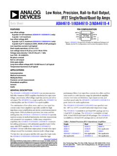
3 The OP482 is available in the PDIP and narrow SOIC packages, as well as a 14-ball WLCSP. PIN CONNECTIONS 12345678 OUT A IN A+IN AV OP-482V+OUT B IN B+IN BOP28200301-001 Figure 1. 8-Lead, Narrow-Body SOIC (S-Suffix) [R-8] 00301-002 OUT A1 IN A2+IN A3V 4V+8 OUT B7 IN B6+IN B5OP282 TOP VIEW(Not to Scale) Figure 2. 8-Lead MSOP [RM-8] 1234567141312111098 OUT A IN A+IN AV++IN B IN BOUT BOUT D IN D+IN DV +IN C IN COUT COP482 ++ ++ 00301-003 Figure 3. 14-Lead PDIP (P-Suffix) [N-14] 1234567141312111098 OUT A IN A+IN AV++IN B IN BOUT BOUT D IN D+IN DV +IN C IN COUT COP48200301-004 Figure 4. 14-Lead, Narrow-Body SOIC (S-Suffix) [R-14] TOP VIEW (BALL SIDE DOWN)Not to Scale00301-048 BALL A1 CORNEROUT A+IN DV +IN COUT COUT D IN AV+ IN BOUT B IN D+IN A+IN B IN CABCDEF123 GHJ Figure 5. 14-Ball WLCSP [CB-14-2] OP282/OP482 Data Sheet Rev.
4 I | Page 2 of 16 TABLE OF CONTENTS Features .. 1 Applications .. 1 General Description .. 1 Pin Connections .. 1 Revision History .. 2 Specifications .. 3 Electrical Characteristics .. 3 Absolute Maximum Ratings .. 4 Thermal Resistance .. 4 ESD Typical Performance Characteristics ..5 Applications Information .. 12 High-Side Signal Conditioning .. 12 Phase Inversion .. 12 Active Filters .. 12 Programmable State Variable Filter .. 13 Outline Dimensions .. 14 Ordering Guide .. 16 REVISION HISTORY 9/13 Rev. H to Rev. I Changes to Figure 5 .. 1 Updated Outline Dimensions .. 14 Changes to Ordering Guide .. 16 9/ 10 Rev. G to Rev. H Added WLCSP .. Universal Changes to Features 1 Changes to General Description Section .. 1 Added Figure 5; Renumbered Sequentially .. 1 Changes to Large-Signal voltage Gain Parameter, Table 1.
5 3 Changes to Table 2, Thermal Resistance Section, and Ta b l e 3 .. 4 Change to Figure 30 .. 9 Added Figure 53 .. 16 Changes to Ordering Guide .. 16 7/08 R e v. F t o R e v. G Changes to Phase Inversion Section .. 12 Deleted Figure 45 .. 12 Added Figure 45 and Figure 12 Updated Outline Dimensions .. 14 Changes to Ordering Guide .. 16 10/04 Rev. E to Rev. F Deleted 8-Lead PDIP .. Universal Added 8-Lead MSOP .. Universal Changes to Format and Layout .. Universal Changes to Features .. 1 Changes to Pin Configurations .. 1 Changes to General Description .. 1 Changes to Specifications .. 3 Changes to Absolute Maximum Ratings .. 4 Changes to Table 3 .. 4 Added Figure 5 through Figure 20; Renumbered Successive Figures .. 5 Updated Figure 21 and Figure 22 .. 7 Updated Figure 23 and Figure 27 .. 8 Updated Figure 29.
6 9 Updated Figure 35 and Figure 36 .. 10 Updated Figure 43 .. 11 Changes to Applications Information .. 12 Changes to Figure 44 .. 12 Deleted OP282/OP482 Spice Macro Model Section .. 9 Deleted Figure 4 .. 9 Deleted OP282 Spice Marco Model .. 10 Updated Outline Dimensions .. 14 Changes to Ordering Guide .. 14 10/02 R e v. D t o R e v. E Edits to 8-Lead Epoxy DIP (P-Suffix) Pin .. 1 Edits to Ordering Guide .. 3 Edits to Outline Dimensions .. 11 9/02 R e v. C t o R e v. D Edits to 14-Lead SOIC (S-Suffix) Pin .. 1 Replaced 8-Lead SOIC (S-Suffix) .. 11 4/02 R e v. B t o R e v. C Wafer Test Limits Deleted .. 2 Edits to Absolute Maximum Ratings .. 3 Dice Characteristics Deleted .. 3 Edits to Ordering Guide .. 3 Edits to Figure 1 .. 7 Edits to Figure 3 .. 8 20-Position Chip Carrier (RC Suffix) Deleted.
7 11 Data Sheet OP282/OP482 Rev. I | Page 3 of 16 SPECIFICATIONS ELECTRICAL CHARACTERISTICS At VS = V, TA = 25 C, unless otherwise noted; applies to both A and G grades. Table 1. Parameter Symbol Test Conditions/Comments Min Typ Max Unit INPUT CHARACTERISTICS Offset voltage VOS OP282 3 mV OP282, 40 C TA +85 C mV OP482 4 mV OP482, 40 C TA +85 C 6 mV Input Bias Current IB VCM = 0 V 3 100 pA VCM = 0 V1 500 pA Input Offset Current IOS VCM = 0 V 1 50 pA VCM = 0 V1 250 pA Input voltage Range 11 +15 V Common-Mode Rejection Ratio CMRR 11 V VCM +15 V, 40 C TA +85 C 70 90 dB Large-Signal voltage Gain AVO RL = 10 k , VO = V 20 V/mV RL = 10 k , 40 C TA +85 C 15 V/mV Offset voltage Drift VOS/ T 10 V/ C Bias Current Drift IB/ T 8 pA/ C OUTPUT CHARACTERISTICS Output voltage High VOH RL = 10 k V Output voltage Low VOL RL = 10 k V Short-Circuit Limit ISC Source 3 10 mA Sink 12 8 mA Open-Loop Output Impedance ZOUT f = 1 MHz 200 power SUPPLY power Supply Rejection Ratio PSRR VS = V to 18 V, 40 C TA +85 C 25 316 V/V Supply Current/ amplifier ISY VO = 0 V.
8 40 C TA 85 C 210 250 A Supply voltage Range VS 18 V DYNAMIC PERFORMANCE Slew Rate SR RL = 10 k 7 9 V/ s Full- power Bandwidth BWP 1% distortion 125 kHz Settling Time tS To s Gain Bandwidth Product GBP 4 MHz Phase Margin M 55 Degrees NOISE PERFORMANCE voltage Noise en p-p Hz to 10 Hz V p-p voltage Noise Density en f = 1 kHz 36 nV/ Hz Current Noise Density in pA/ Hz 1 The input bias and offset currents are characterized at TA = TJ = 85 C. Bias and offset currents are guaranteed but not tested at 40 C. OP282/OP482 Data Sheet Rev. I | Page 4 of 16 ABSOLUTE MAXIMUM RATINGS Table 2. Parameter Rating Supply voltage 18 V Input voltage 18 V Differential Input Voltage1 36 V Output Short-Circuit Duration Indefinite Storage Temperature Range 65 C to +150 C Operating Temperature Range 40 C to +85 C Junction Temperature Range 65 C to +150 C Lead Temperature (Soldering 60 sec) 300 C 1 For supply voltages less than 18 V, the absolute maximum input voltage is equal to the supply voltage .
9 Stresses above those listed under Absolute Maximum Ratings may cause permanent damage to the device. This is a stress rating only; functional operation of the device at these or any other conditions above those indicated in the Operational section of this specification is not implied. Exposure to absolute maximum rating conditions for extended periods may affect device reliability. THERMAL RESISTANCE JA is specified for the worst-case conditions, that is, a device in socket for PDIP. JA is specified for a device soldered in the circuit board for SOIC_N, MSOP, and WLCSP packages. This was measured using a standard 4-layer board. Table 3. Package Type JA JC Unit 8-Lead MSOP [RM] 142 45 C/W 8-Lead SOIC_N (S-Suffix) [R] 120 45 C/W 14-Lead PDIP (P-Suffix) [N] 83 39 C/W 14-Lead SOIC_N (S-Suffix) [R] 112 35 C/W 14-Ball WLCSP [CB]1, 2 70 16 C/W 1 Simulated thermal numbers per JESD51-9.
10 2 Junction-to-board thermal resistance. ESD CAUTION Data Sheet OP282/OP482 Rev. I | Page 5 of 16 TYPICAL PERFORMANCE CHARACTERISTICS FREQUENCY (Hz)OPEN-LOOP GAIN (dB)1k 40 20608010k1M10M00301-005100k20400VS = 15 VTA = 25 CPHASE (Degrees) 4513545900 90180 Figure 6. OP282 Open-Loop Gain and Phase vs. Frequency TEMPERATURE ( C)OPEN-LOOP GAIN (V/mV) 75053545 2510012500301-00625152510VS = 15 VRL = 10k 20304075500 50 Figure 7. OP282 Open-Loop Gain vs. Temperature LOAD CAPACITANCE (pF)OVERSHOOT (%)0010708020040050000301-00730502040603 00100VS = 15 VRL = 2k VIN = 100mV p-pAVCL= 1TA = 25 C+OS OS Figure 8. OP282 Small-Signal Overshoot vs. Load Capacitance FREQUENCY (Hz)CLOSED-LOOP GAIN (dB)1k 30 20607010k1M10M00301-008100k20400VS = 15 VTA = 25 C 10501030 AVCL= 100 AVCL= 10 AVCL= 1 Figure 9. OP282 Closed-Loop Gain vs. Frequency TEMPERATURE ( C)SLEW RATE (V/ s) 750530 2510012500301-00925152510VS = 15 VRL = 10k CL = 50pF2075500 50 SR+SR Figure 10.