Transcription of Dual Very Low Noise Precision Operational …
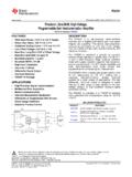
1 Dual Very Low Noise Precision Operational Amplifier Data Sheet OP270. FEATURES FUNCTIONAL BLOCK DIAGRAMS. Very low Noise density of 5 nV/ Hz at 1 kHz maximum IN A 1 16 OUT A. Excellent input offset voltage of 75 V maximum +IN A 2 15 NC. Low offset voltage drift of 1 V/ C maximum NC 3 14 NC. V 4 13 V+. Very high gain of 1500 V/mV minimum OP270. NC 5 12 NC. Outstanding CMR of 106 dB minimum +IN B 6 11 NC. Slew rate of V/ s typical IN B 7 10 OUT B. Gain bandwidth product of 5 MHz typical NC 8 9 NC. 00325-001. Industry-standard 8-lead dual pinout NC = NO CONNECT.
2 Figure 1. 16-Lead SOIC. (S-Suffix). OUT A 1 8 V+. IN A 2 A B 7 OUT B. +IN A 3 6 IN B. 00325-002. V 4 5 +IN B. OP270. Figure 2. 8-Lead PDIP (P-Suffix). 8-Lead CERDIP. (Z-Suffix). GENERAL DESCRIPTION. The OP270 is a high performance, monolithic, dual Operational consumption of the dual OP270 is one-third less than two OP27. amplifier with exceptionally low voltage Noise density (5 nV/ Hz devices , a significant advantage for power conscious applications. maximum at 1 kHz). It offers comparable performance to the The OP270 is unity-gain stable with a gain bandwidth product industry-standard OP27 from analog devices , Inc.
3 Of 5 MHz and a slew rate of V/ s. The OP270 features an input offset voltage of less than 75 V The OP270 offers excellent amplifier matching, which is and an offset drift of less than 1 V/ C, guaranteed over the full important for applications such as multiple gain blocks, low military temperature range. Open-loop gain of the OP270 is more Noise instrumentation amplifiers, dual buffers, and low Noise than 1,500,000 into a 10 k load, ensuring excellent gain accuracy active filters. and linearity, even in high gain applications.
4 The input bias The OP270 conforms to the industry-standard 8-lead CERDIP. current is less than 20 nA, which reduces errors due to signal and PDIP pinouts. source resistance. With a common-mode rejection (CMR) of greater than 106 dB and a power supply rejection ratio (PSRR) For higher speed applications, the ADA4004-2 or the AD8676. of less than V/V, the OP270 significantly reduces errors are recommended. For a quad op amp, see the OP470 data sheet. due to ground Noise and power supply fluctuations. The power Rev. F Document Feedback Information furnished by analog devices is believed to be accurate and reliable.
5 However, no responsibility is assumed by analog devices for its use, nor for any infringements of patents or other rights of third parties that may result from its use. Specifications subject to change without notice. No One Technology Way, Box 9106, Norwood, MA 02062-9106, license is granted by implication or otherwise under any patent or patent rights of analog devices . Tel: 2001 2015 analog devices , Inc. All rights reserved. Trademarks and registered trademarks are the property of their respective owners. Technical Support OP270 Data Sheet TABLE OF CONTENTS.
6 Features .. 1 Voltage and Current Noise .. 12 Functional Block Diagrams .. 1 Total Noise and Source Resistance .. 12 General Description .. 1 Noise Measurements .. 14 Revision History .. 2 Capacitive Load Driving and Power Supply Considerations .. 15 3 Unity-Gain Buffer Applications .. 15 Electrical Specifications .. 4 Low Phase Error Amplifier .. 16 Absolute Maximum 5 Five-Band, Low Noise , Stereo Graphic Equalizer .. 16 ESD Caution .. 5 Digital Panning Control .. 17 Typical Performance Characteristics .. 6 Dual Programmable Gain Amplifier.
7 17 Test Circuits .. 11 Outline Dimensions .. 19 Applications Information .. 12 Ordering Guide .. 20 REVISION HISTORY. 10/15 Rev. E to Rev. F 4/03 Rev. B to Rev. C. Changes to General Description Section .. 1 Deletion of OP270A model .. Universal Changes to Supply Voltage Parameter and Differential Input Edits to Voltage Parameter, Table 3 .. 5 Changes to Specifications ..2. Deleted Table 4; Renumbered Sequentially .. 5 Deletion of Wafer Limits and Dice Characteristics ..4. Changes to Absolute Maximum Ratings ..4. 2/10 Rev.
8 D to Rev. E Changes to Ordering Guide ..4. Change to Input Noise Current Density Parameter, Table 1 .. 3 Changes to Equations in Noise Measurements 10. Change to Figure 18 .. 8 Change to Figure 10 .. 11. Updated Outline Dimensions .. 14. 2/09 Rev. C to Rev. D. Updated Format .. Universal 11/02 Rev. A to Rev. B. Reorganized Layout .. Universal Updated Ordering Guide .. 15. Changes to Figure 7 .. 6. Changes to Figure 22 .. 9 9/02 Rev. 0 to Rev. A. Deleted Applications Heading .. 11 Edits to Absolute Maximum Ratings ..5. Changes to Figure 44.
9 17 Edits to Ordering Guide .. 15. Changes to Figure 46 .. 18. Updated Outline Dimensions .. 19 2/01 Revision 0: Initial Version Changes to Ordering Guide .. 20. Rev. F | Page 2 of 20. Data Sheet OP270. SPECIFICATIONS. VS = 15 V, TA = 25 C, unless otherwise noted. Table 1. OP270E OP270F OP270G. Parameter Symbol Test Conditions Min Typ Max Min Typ Max Min Typ Max Unit Input Offset Voltage VOS 10 75 20 150 50 250 V. Input Offset Current IOS VCM = 0 V 1 10 3 15 5 20 nA. Input Bias Current IB VCM = 0 V 5 20 10 40 15 60 nA. Input Noise Voltage1 en p-p Hz to 10 Hz 80 200 80 200 80 nV p-p Input Noise Voltage Density2 en fO = 10 Hz nV/ Hz en fO = 100 Hz nV/ Hz en fO = 1 kHz nV/ Hz Input Noise Current Density in fO = 10 Hz pA/ Hz in fO = 100 Hz pA/ Hz in fO = 1 kHz pA/ Hz Large-Signal Voltage Gain AVO VO = 10 V, 1500 2300 1000 1700 750 1500 V/mV.
10 RL = 10 k . VO = 10 V, 750 1200 500 900 350 700 V/mV. RL = 2 k . Input Voltage Range3 IVR 12 12 12 V. Output Voltage Swing VO RL 2 k 12 12 12 V. Common-Mode Rejection CMR VCM = 11 V 106 125 100 120 90 110 dB. Power Supply Rejection PSRR VS = V V/V. Ratio to 18 V. Slew Rate SR V/ s Supply Current ISY No load 4 4 4 mA. (All Amplifiers). Gain Bandwidth Product GBP 5 5 5 MHz Channel Separation1 CS VO = 20 V p-p, 125 175 125 175 175 dB. fO = 10 Hz Input Capacitance CIN 3 3 3 pF. Input Resistance Differential Mode RIN M . Common Mode RINCM 20 20 20 G.