Transcription of EEPROM Serial 2/4/8/16Kb IC - ON Semiconductor
1 DATA Semiconductor Components Industries, LLC, 2016 July, 2022 Rev. 361 Publication Order Number:CAT24C01/DEEPROM Serial 2/4/8/16 Kb I2 CCAT24C02, CAT24C04,CAT24C08, CAT24C16 DescriptionThe CAT24C02/04/08/16 are 2 Kb, 4 Kb, 8 Kb and 16 Kbrespectively I2C Serial EEPROM devices organized internally as16/32/64 and 128 pages respectively of 16 bytes each. All devicessupport both the Standard (100 kHz) as well as Fast (400 kHz) is written by providing a starting address, then loading 1 to 16contiguous bytes into a Page Write Buffer, and then writing all data tonon volatile memory in one internal write cycle.
2 Data is read byproviding a starting address and then shifting out data serially whileautomatically incrementing the internal address address pins make it possible to address up to eightCAT24C02, four CAT24C04, two CAT24C08 and one CAT24C16device on the same Supports Standard and Fast I2C Protocol V to V Supply Voltage Range 16 Byte Page Write Buffer Hardware Write Protection for Entire Memory Schmitt Triggers and Noise Suppression Filters on I2C Bus Inputs(SCL and SDA) Low power CMOS Technology More than 1,000,000 Program/Erase Cycles 100 Year Data Retention Industrial and Extended Temperature Range These Devices are Pb Free.
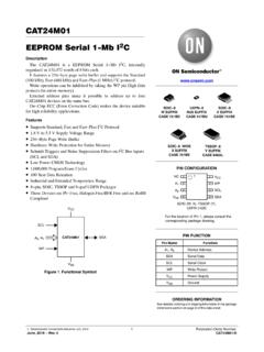
3 Halogen Free/BFR Free and are RoHSCompliantThis document contains information on some products that are still under reserves the right to change or discontinue these products without 8W SUFFIXCASE 751 BDTSOT 23TD SUFFIXCASE 419 AETSSOP 8Y SUFFIXCASE 948 ALUDFN8 EPHU4 SUFFIXCASE 517 AZWLCSP 4**C4A SUFFIXCASE 567 DCWLCSP 5**C5A SUFFIXCASE 567 DDSee detailed ordering and shipping information in the packagedimensions section on page 10 of this data INFORMATIONWLCSP 4**C4U SUFFIXCASE 567 NXFor Serial EEPROM in the US8 package, please consult the N24C02 datasheet** WLCSP are available for the CAT24C04, CAT24C08 and CAT24C16 , CAT24C04, CAT24C08, CONFIGURATIONS AND MARKING INFORMATIONSCLWPCAT24 CxxFigure 1.
4 Functional SymbolVSSSDAVCCA2, A1, A0 Table 1. PIN FUNCTIONPin Name FunctionA0, A1, A2 Device Address InputSDAS erial Data Input/OutputSCLS erial Clock InputWPWrite Protect InputVCCP ower SupplyVSSG roundNCNo Connect The exposed pad for the UDFN packages can be left floating orconnected to 23 (TD) (Top View)** WLCSP are available for the CAT24C04, CAT24C08 and CAT24C16 MARKING FOR WLCSPX = Specific DeviceX = Code4 or R = 24C048 or T = 24C086 or V = 24C16Y = Production Year (Last Digit)M = Production Month (1 9, O, N, D)W = Production WeekWLCSP 4(C4A)WLCSP 5 WLCSP 4**WLCSP 5**(Top Views)WPSCLSDASCLSDAPin 1A12 312 BCABPin 1 VCCVSSVCCVSS X XY MY MPin 1(Ball Down)
5 Pin 1 SDASCLWPVCCVSS12348765 CAT24C__16 / 08 / 04 / 02NC///NC NCNC NCNCA0A1A1A2A2A2//////SOIC (W), TSSOP (Y),UDFN EP (HU4) (Top View)WLCSP 4(C4U) XY WPin 1 CAT24C02, CAT24C04, CAT24C08, 2. ABSOLUTE MAXIMUM RATINGSP arametersRatingsUnitsStorage Temperature 65 to +150 CVoltage on any pin with respect to Ground (Note 1) to + exceeding those listed in the Maximum Ratings table may damage the device. If any of these limits are exceeded, device functionalityshould not be assumed, damage may occur and reliability may be During input transitions, voltage undershoot on any pin should not exceed 1 V for more than 20 ns. Voltage overshoot on pins A0, A1, A2and WP should not exceed VCC + 1 V for more than 20 ns, while voltage on the I2C bus pins, SCL and SDA, should not exceed the absolutemaximum ratings, irrespective of 3.
6 RELIABILITY CHARACTERISTICS (Note 2)SymbolParameterMinUnitsNEND (Note 3)Endurance1,000,000 Program / Erase CyclesTDRData Retention100 Years2. These parameters are tested initially and after a design or process change that affects the parameter according to appropriate AEC Q100and JEDEC test Page Mode, VCC = 5 V, 25 4. OPERATING CHARACTERISTICS(VCC = V to V, TA = 40 C to +125 C and VCC = V to V, TA = 40 C to +85 C, unless otherwise specified.)SymbolParameterTest ConditionsMinMaxUnitsICCR Read CurrentRead, fSCL = 400 kHz1mAICCW Write CurrentWrite, fSCL = 400 kHz2mAISBS tandby CurrentAll I/O Pins at GND or VCCTA = 40 C to +85 CVCC V1mATA = 40 C to +85 CVCC > V3TA = 40 C to +125 C5 ILI/O Pin LeakagePin at GND or VCC2mAVIL Input Low Voltage x VCCVVIH Input High VoltageA0, A1, A2 and x VCCVCC + and x output LowVoltageVCC > V, IOL = 3 < V, IOL = 1 parametric performance is indicated in the Electrical Characteristics for the listed test conditions, unless otherwise noted.
7 Productperformance may not be indicated by the Electrical Characteristics if operated under different , CAT24C04, CAT24C08, 5. PIN IMPEDANCE CHARACTERISTICS(VCC = V to V, TA = 40 C to +125 C and VCC = V to V, TA = 40 C to +85 C, unless otherwise specified.)SymbolParameterConditionsMaxU nitsCIN (Note 4) SDA Pin CapacitanceVIN = 0 V, f = MHz, VCC = V8pF Other Pins6pFIWP (Note 5) WP Input CurrentVIN < VIH, VCC = V130mAVIN < VIH, VCC = V120 VIN < VIH, VCC = V80 VIN > VIH2IA (Note 5) Address Input Current (A0, A1, A2) Product Rev H: CAT24C02 Product Rev K: CAT24C04, CAT24C08, CAT24C16 VIN < VIH, VCC = V50mAVIN < VIH, VCC = V35 VIN < VIH, VCC = V25 VIN > VIH24.
8 These parameters are tested initially and after a design or process change that affects the parameter according to appropriate AEC Q100and JEDEC test When not driven, the WP, A0, A1 and A2 pins are pulled down to GND internally. For improved noise immunity, the internal pull down isrelatively strong; therefore the external driver must be able to supply the pull down current when attempting to drive the input HIGH. Toconserve power, as the input level exceeds the trip point of the CMOS input buffer (~ x VCC), the strong pull down reverts to a weakcurrent 6. CHARACTERISTICS(Note 6) (VCC = V to V, TA = 40 C to +125 C and VCC = V to V, TA = 40 C to +85 C, unless otherwise specified.)
9 SymbolParameterStandardFastUnitsMinMaxMi nMaxFSCLC lock Frequency100400kHztHD:STASTART Condition Hold Period of SCL Period of SCL :STASTART Condition Setup :DATData In Hold Time00mstSU:DATData In Setup Time250100nstRSDA and SCL Rise Time1000300nstF (Note 6)SDA and SCL Fall Time300300nstSU:STOSTOP Condition Setup Free Time Between STOP and Low to Data Out Out Hold Time100100nsTi (Note 6)Noise Pulse Filtered at SCL and SDA Inputs100100nstSU:WPWP Setup Time00mstHD:WPWP Hold Cycle Time55mstPU (Notes 7, 8)Power up to Ready Mode11ms6. Test conditions according to AC Test Conditions Tested initially and after a design or process change that affects this tPU is the delay between the time VCC is stable and the device is ready to accept , CAT24C04, CAT24C08, 7.
10 TEST CONDITIONSI nput Drive x VCC to x VCCI nput Rise and Fall Timev 50 nsInput Reference x VCC, x VCCO utput Reference x VCCO utput Test LoadCurrent Source IOL = 3 mA (VCC w V); IOL = 1 mA (VCC < V); CL = 100 pFPower On Reset (POR)Each CAT24 Cxx* incorporates Power On Reset (POR)circuitry which protects the internal logic against poweringup in the wrong CAT24 Cxx device will power up into Standby modeafter VCC exceeds the POR trigger level and will powerdown into Reset mode when VCC drops below the PORtrigger level. This bi directional POR feature protects thedevice against brown out failure following a temporaryloss of power.