Transcription of Efficiency of Buck Converter - Rohm
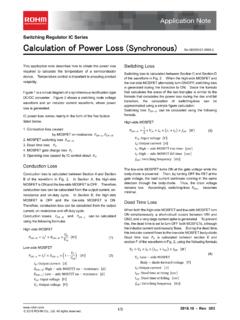
1 1/15 2016, 2021 ROHM Co., Ltd. No. 64AN035E APRIL 2021 Application Note switching Regulator IC Series Efficiency of buck Converter switching regulators are known as being highly efficient power sources. To further improve their Efficiency , it is helpful to understand the basic mechanism of power loss. This application note explains power loss factors and methods for calculating them. It also explains how the relative importance of power loss factors depends on the specifications of the switching power source. Synchronous rectification type Figure 1 shows the circuit diagram of a synchronous rectification type DC/DC Converter .
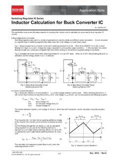
2 Figure 2 shows the waveforms of the voltage of a switch node and the current waveform of the inductor. The striped patterns represent the areas where the loss occurs. The following nine factors are the main causes of power loss: 1. Conduction loss caused by the on-resistance of the MOSFET , 2. switching -loss in the MOSFET , 3. Reverse recovery loss in the body diode 4. Output capacitance loss in the MOSFET 5. Dead time loss 6. Gate charge loss in the MOSFET 7. Operation loss caused by the IC control circuit 8.
3 Conduction loss in the inductor ( ) 9. Loss in the capacitor , Conduction loss in the MOSFET The conduction loss in the MOSFET is calculated in the A and B sections of the waveform in Figure 2. As the high-side MOSFET is ON and the low-side MOSFET is OFF in the A section, the conduction loss of the high-side MOSFET can be estimated from the output current, on-resistance, and on-duty cycle. As the high-side MOSFET is OFF and the low-side MOSFET is ON in the B section, the conduction loss of the low-side MOSFET can be estimated from the output current, on-resistance, and off-duty cycle.
4 The conduction losses and are calculated with the following equations. High-side MOSFET = 2 [ ] Low-side MOSFET = 2 (1 ) [ ] : Output current [ ] : High-side MOSFET on-resistance [ ] : Low-side MOSFET on-resistance [ ] : Input voltage [ ] : Output voltage [ ] In the equations (1) and (2), the output current is used as the current value. This is the average current of the inductor. As shown in the lower part of Figure 2, greater losses are generated in the actual ramp waveforms.
5 If the current waveform is sharper (peak current is higher), the effective current is obtained by integrating the square of the differential between the peak and bottom values of the current. The loss can then be calculated in more detail. The conduction losses and are calculated with the following equations. High-side MOSFET =[ 2+( )212] [ ] (1) (2) (3) 2/15 2016, 2021 ROHM Co., Ltd. No. 64AN035E APRIL 2021 Application Note Efficiency of buck Converter Low-side MOSFET =[ 2+( )212] (1 ) [ ] =( ) [ ] = + 2 [ ] = : Output current [ ] : Inductor current peak [ ] : Inductor current bottom [ ] : High-side MOSFET on-resistance [ ] : Low-side MOSFET on-resistance [ ] : Input voltage [ ] : Output voltage [ ] : Ripple current of inductor [ ] : switching frequency [ ].
6 Inductance value [ ] switching -loss in the MOSFET The switching -losses are calculated in the C and D sections or in the E and F sections of the waveform in Figure 2. When the high-side and low-side mosfets are turned ON and OFF alternately, a loss is generated during the transition of the on- switching . Since the equation for calculating the area of the two triangles is similar to the equation for calculating the power losses during the rising and falling transitions, this calculation can be approximated using a simple geometric equation.
7 The switching -loss is calculated with the following equation. High-side MOSFET =12 ( + ) [ ] : Input voltage [ ] : Output current [ ] : High-side MOSFET rise time [ ] : High-side MOSFET rise time [ ] : switching frequency [ ] When the low-side MOSFET is turned ON by the gate voltage while the body diode is energized and then the FET is turned OFF by the gate voltage, the load current continues to flow in the same direction through the body diode. Therefore, the drain voltage becomes equal to the forward direction voltage and remains low.
8 Then, the resulting switching -loss is very small, as described in the following equation. Low-side MOSFET =12 ( + ) [ ] : Forward direction voltage of low-side MOSFET body diode [ ] : Output current [ ] : Low-side MOSFET rise time [ ] : Low-side MOSFET rise time [ ] : switching frequency [ ] Reverse recovery loss in the body diode When the high-side MOSFET is turned ON, the transition of the body diode of the low-side MOSFET from the forward direction to the reverse bias state causes a diode recovery, which in turn generates a reverse recovery loss in the body diode.
9 This loss is determined by the reverse recovery time of the diode . From the reverse recovery properties of the diode, the loss is calculated with the following equation. =12 [ ] : Input voltage [ ] : Peak value of body diode reverse recovery current [ ] : Body diode reverse recovery time : switching frequency [ ] Output capacitance loss in the MOSFET In each switching cycle, the loss is generated because the output capacitances of the high-side and low-side mosfets are charged.
10 This loss is calculated with the following equation. (5) (6) (7) (4) 3/15 2016, 2021 ROHM Co., Ltd. No. 64AN035E APRIL 2021 Application Note Efficiency of buck Converter =12 ( + ) 2 [ ] = + [ ] = + [ ] : Low-side MOSFET output capacitance [ ] : Low-side MOSFET drain-source capacitance [ ] : Low-side MOSFET gate-drain capacitance [ ] : High-side MOSFET output capacitance [ ] : High-side MOSFET drain-source capacitance [ ] : High-side MOSFET gate-drain capacitance [ ] : Input voltage [ ].