Transcription of ESD7424 - Ultra-Low Capacitance ESD Protection
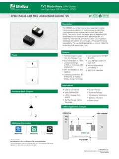
1 Semiconductor Components Industries, LLC, 2016 June, 2017 Rev. 01 Publication Order Number: ESD7424 /DESD7424 Ultra-Low Capacitance ESDP rotectionMicro Packaged Diodes for ESD ProtectionThe ESD7424 is designed to protect voltage sensitive componentsthat require ultra low Capacitance from ESD and transient voltageevents. It has industry leading Capacitance linearity over voltagemaking it ideal for RF applications. This Capacitance linearitycombined with the extremely small package and low insertion lossmakes this part well suited for use in antenna line applications forwireless handsets and Industry Leading Capacitance Linearity Over Voltage ultra Low Capacitance : < pF Max Insertion Loss: dB at 1 GHz; dB at 3 GHz Low Leakage: < 1 mA Protection for the following IEC Standards: IEC61000 4 2 (ESD): Level 4 30 kV Contact ISO 10605 (ESD) 330 pF/330 W 30 kV Contact SZ Prefix for Automotive and Other Applications Requiring UniqueSite and Control Change Requirements.
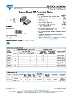
2 AEC Q101 Qualified andPPAP Capable These Devices are Pb Free, Halogen Free/BFR Free and are RoHSCompliantTypical Applications RF Signal ESD Protection Automotive Antenna ESD Protection Near Field Communications USB , USB RATINGS (TA = 25 C unless otherwise noted)RatingSymbolValueUnitIEC 61000 4 2 Contact (Note 1)IEC 61000 4 2 AirISO 10605 Contact (330 pF / 330 W)ISO 10605 Contact (330 pF / 2 kW)ISO 10605 Contact (150 pF / 2 kW)ESD 30 30 30 30 30kVkVkVkVkVTotal Power Dissipation (Note 2) @ TA = 25 CThermal Resistance, Junction to Ambient PD RqJA300400mW C/WJunction and Storage Temperature RangeTJ, Tstg 55 to+150 CLead Solder Temperature Maximum(10 Second Duration)TL260 CStresses exceeding those listed in the Maximum Ratings table may damage thedevice. If any of these limits are exceeded, device functionality should not beassumed, damage may occur and reliability may be Non repetitive current pulse at TA = 25 C, per IEC61000 4 2 Mounted with recommended minimum pad size, DC board FR 4 DevicePackageShipping ORDERING For information on tape and reel specifications,including part orientation and tape sizes, pleaserefer to our Tape and Reel Packaging SpecificationsBrochure, BRD8011 (Pb Free)8000 / Tape &ReelMARKINGDIAGRAMK= Specific Device CodeM= Date CodeUDFN2 CASE 517 CZSZESD7424 MUT5 GUDFN2(Pb Free)8000 / Tape & CHARACTERISTICS(TA = 25 C unless otherwise noted)
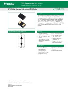
3 SymbolParameterIPPM aximum Reverse Peak Pulse CurrentVCClamping Voltage @ IPPVRWMW orking Peak Reverse VoltageIRMaximum Reverse Leakage Current @ VRWMVBRB reakdown Voltage @ ITITTest Current*See Application Note AND8308/D for detailed explanations ofdatasheet Directional TVSIPPIPPVIIRITITIRVRWMVCVBRVRWMVCVBRELE CTRICAL CHARACTERISTICS (TA = 25 C unless otherwise noted)ParameterSymbolConditionMinTypMaxU nitReverse Working VoltageVRWM24 VBreakdown VoltageVBRIT = 1 mA (Note 3)2630 VReverse Leakage CurrentIRVRWM = 24 Voltage TLPVCIPP = 8 A (Note 4)IPP = 16 A (Note 4)3845 VJunction CapacitanceCJVR = 0 V, f = 1 MHzVR = 0 V, f = 1 ResistanceRDYNTLP Lossf = 1 GHzf = 3 parametric performance is indicated in the Electrical Characteristics for the listed test conditions, unless otherwise noted. Productperformance may not be indicated by the Electrical Characteristics if operated under different Breakdown voltage is tested from pin 1 to 2 and pin 2 to ANSI/ESD Electrostatic Discharge Sensitivity Testing using Transmission Line Pulse (TLP) Model.
4 TLP conditions: Z0 = 50 W, tp = 100 ns, tr = 4 ns, averaging window; t1 = 30 ns to t2 = 60 1. IEC61000 4 2 +8 kV Contact ESDC lamping VoltageFigure 2. IEC61000 4 2 8 kV Contact ESDC lamping VoltageTIME (ns)TIME (ns)1501251007550250 25 20020601001201601501251007550250 25 160 120 100 80 40020 VOLTAGE (V)VOLTAGE (V)1754080140175 140 60 CHARACTERISTICSF igure 3. Typical IV CharacteristicsFigure 4. Typical CV CharacteristicsVOLTAGE (V)VOLTAGE (V)4030100 10 11168240 8 16 5. Typical Insertion LossESD7424 MUT5 GFigure 6. Typical Capacitance over FrequencyESD7424 MUT5 GFREQUENCY (Hz)FREQUENCY (Hz) + +07 10 8 7 4 3 + + + + (A) Capacitance (pF)s21 (dB) Capacitance (pF)20 30 4 12 20f = 1 + +10 2 5 6 9VR = 0 61000 4 2 Volt-age (kV)First PeakCurrent(A)Current at30 ns (A)Current at60 ns (A) 4 2 Waveform100%I @ 30 nsI @ 60 nstP = ns to 1 nsFigure 7.
5 IEC61000 4 2 SpecFigure 8. Diagram of ESD Clamping Voltage Test Setup50 W50 WCableTVSO scilloscopeESD GunThe following is taken from Application NoteAND8308/D Interpretation of Datasheet Parametersfor ESD Voltage ClampingFor sensitive circuit elements it is important to limit thevoltage that an IC will be exposed to during an ESD eventto as low a voltage as possible. The ESD clamping voltageis the voltage drop across the ESD Protection diode duringan ESD event per the IEC61000 4 2 waveform. Since theIEC61000 4 2 was written as a pass/fail spec for largersystems such as cell phones or laptop computers it is notclearly defined in the spec how to specify a clamping voltageat the device level. ON Semiconductor has developed a wayto examine the entire voltage waveform across the ESDprotection diode over the time domain of an ESD pulse in theform of an oscilloscope screenshot, which can be found onthe datasheets for all ESD Protection diodes.
6 For moreinformation on how ON Semiconductor creates thesescreenshots and how to interpret them please refer toAND8307 9. Positive TLP I V CurveFigure 10. Negative TLP I V CurveNOTE:TLP parameter: Z0 = 50 W, tp = 100 ns, tr = 300 ps, averaging window: t1 = 30 ns to t2 = 60 ns. VIEC is the equivalent voltagestress level calculated at the secondary peak of the IEC 61000 4 2 waveform at t = 30 ns with 2 A/kV. See TLP descriptionbelow for more CURRENT (A)VC, VOLTAGE (V)0246810121416010203040500246105152535 45 EQUIVALENT VIEC (kV)TLP CURRENT (A)VC, VOLTAGE (V)0 2 4 6 8 10 12 14 1601020304050024610515253545 EQUIVALENT VIEC (kV)18208 18 208 Transmission Line Pulse (TLP) MeasurementTransmission Line Pulse (TLP) provides current versusvoltage (I V) curves in which each data point is obtainedfrom a 100 ns long rectangular pulse from a chargedtransmission line.
7 A simplified schematic of a typical TLPsystem is shown in Figure 11. TLP I V curves of ESDprotection devices accurately demonstrate the product sESD capability because the 10s of amps current levels andunder 100 ns time scale match those of an ESD event. Thisis illustrated in Figure 12 where an 8 kV IEC 61000 4 2current waveform is compared with TLP current pulses at8 A and 16 A. A TLP I V curve shows the voltage at whichthe device turns on as well as how well the device clampsvoltage over a range of current 11. Simplified Schematic of a Typical TLPS ystemDUTLS OscilloscopeAttenuator10 MWVCVMIM50 W CoaxCable50 W CoaxCableFigure 12. Comparison Between 8 kV IEC 61000 4 2 and 8 A and 16 A TLP WaveformsUDFN2 , 517 CZISSUE DDATE 02 JUL 2020 SCALE 4:1XX= Specific Device CodeM= Date CodeGENERICMARKING DIAGRAM**This information is generic. Please referto device data sheet for actual partmarking.
8 Pb Free indicator, G , mayor not be present. Some products maynot follow the Generic CASE OUTLINEPACKAGE DIMENSIONSON Semiconductor and are trademarks of Semiconductor Components Industries, LLC dba ON Semiconductor or its subsidiaries in the United States and/or other Semiconductor reserves the right to make changes without further notice to any products herein. ON Semiconductor makes no warranty, representation or guarantee regardingthe suitability of its products for any particular purpose, nor does ON Semiconductor assume any liability arising out of the application or use of any product or circuit, and specificallydisclaims any and all liability, including without limitation special, consequential or incidental damages. ON Semiconductor does not convey any license under its patent rights nor therights of NUMBER:DESCRIPTION:Electronic versions are uncontrolled except when accessed directly from the Document versions are uncontrolled except when stamped CONTROLLED COPY in 1 OF 1 UDFN2 , Semiconductor Components Industries, LLC, Semiconductor and are trademarks of Semiconductor Components Industries, LLC dba ON Semiconductor or its subsidiaries in the United States and/or other Semiconductor owns the rights to a number of patents, trademarks, copyrights, trade secrets, and other intellectual property.
9 A listing of ON Semiconductor s product/patentcoverage may be accessed at ON Semiconductor reserves the right to make changes without further notice to any products Semiconductor makes no warranty, representation or guarantee regarding the suitability of its products for any particular purpose, nor does ON Semiconductor assume any liabilityarising out of the application or use of any product or circuit, and specifically disclaims any and all liability, including without limitation special, consequential or incidental is responsible for its products and applications using ON Semiconductor products, including compliance with all laws, regulations and safety requirements or standards,regardless of any support or applications information provided by ON Semiconductor. Typical parameters which may be provided in ON Semiconductor data sheets and/orspecifications can and do vary in different applications and actual performance may vary over time.
10 All operating parameters, including Typicals must be validated for each customerapplication by customer s technical experts. ON Semiconductor does not convey any license under its patent rights nor the rights of others. ON Semiconductor products are notdesigned, intended, or authorized for use as a critical component in life support systems or any FDA Class 3 medical devices or medical devices with a same or similar classificationin a foreign jurisdiction or any devices intended for implantation in the human body. Should Buyer purchase or use ON Semiconductor products for any such unintended or unauthorizedapplication, Buyer shall indemnify and hold ON Semiconductor and its officers, employees, subsidiaries, affiliates, and distributors harmless against all claims, costs, damages, andexpenses, and reasonable attorney fees arising out of, directly or indirectly, any claim of personal injury or death associated with such unintended or unauthorized use, even if suchclaim alleges that ON Semiconductor was negligent regarding the design or manufacture of the part.