Transcription of Fabrication of antiscatter grids and collimators for …
1 TECHNICAL PAPERF abrication of antiscatter grids and collimators for X-rayand gamma-ray imaging by lithography and electroformingOlga V. Makarova Guohua Yang Platte T. Amstutz Cha-Mei TangReceived: 16 July 2007 / Accepted: 3 January 2008 / Published online: 22 January 2008 Springer-Verlag 2008 AbstractCreatv MicroTech has developed unique fab-rication techniques to make high precision, high-aspect-ratio metal microstructures to custom specifications. Alithography based Fabrication method permits precise fab-rication of various microstructures. collimators andantiscatter grids with continuous, smooth, thin, parallel orfocused septa have been fabricated using deep X-ray andoptical lithography , combined with metal of high-aspect-ratio structures, especiallyof relatively large areas, presents many challenges: spe-cialized mask design and X-ray mask Fabrication ; resistpreparation, optimal exposure parameters, post-exposureprocessing, electroforming , polishing, and final , we present microstructures of various designs that wefabricated and describe the challenges that had to IntroductionCreatv MicroTech Inc.
2 (Creatv) has developed fabricationprocesses to make high quality, high-aspect-ratio metalmicrostructures to meet custom specifications. The fabri-cation method is based on lithography that allows precisefabrication of various microstructures. To fabricate themetal parts, we use different resist materials, X-ray or UV- lithography as appropriate, and electroforming or electro-less plating of a variety of metals ( , Cu, Ni, Pb, Ag, andAu). The experience gained over several years allows us tomove from custom design to a completed part in a rela-tively short period of collimator and anti-scatter grid are crucial elementsin determining the sensitivity, resolution, and contrast ofimages in nuclear medicine and X-ray imaging .
3 In order tomaximize the transmission of primary radiation, septawalls must be as thin as possible and be parallel to theprimary radiation. In order to eliminate the transmission ofscattered radiation, the grid must be tall enough and madefrom suitable absorbing metal. To fabricate a metal gridstructure, the resist mold consisting of channels is fabri-cated first. Microfabrication of deep channels, especially ina relatively large resist area, is very challenging and sel-dom reported. In this paper, we present a number ofstrategies to fabricate high-aspect-ratio grids and collima-tors of various MethodLithography and electroforming is a unique method thatallows manufacturing of microstructures with dimensionsfrom several microns to several millimeters with highprecision on a large area.
4 The main steps of the opticallithography method are: Design and fabricate the optical mask on chromium-on-glass substrate. Transfer the pattern from the optical mask to a thickresist layer attached on conductive substrate. Develop the resist, such that the residual resist layerserves as a mold for metal V. Makarova (&) G. YangCreatv MicroTech Inc., Chicago, IL 60612, USAe-mail: T. Amstutz TangCreatv MicroTech Inc., Potomac, MD 20854, USA123 Microsyst Technol (2008) 14:1613 1619 DOI Electroform the part using the developed resist/substrate. Lap and polish the electroformed part, after which theremaining resist mold is removed, resulting in afreestanding metal layer. Stacking, if necessary, of several layers to achieve thedesired height is performed using precise X-ray lithography , an additional step of X-ray maskfabrication is required.
5 We use both optical and X-raylithography for the Fabrication of custom a positive polymethylmethacrylate (PMMA, Good-fellow, CQ-grade) and a negative SU-8 (MicroChem) tonephotoresists have been used. X-ray exposures wereperformed at the wiggler beamline at the Center forAdvanced Microstructures and Devices at Louisiana StateUniversity in Baton Rouge. Optical exposures are per-formed at the Center for Nanoscale Materials of ArgonneNational Laboratory using a Karl Suss MA 6 mask aligner,and at Creatv MicroTech using a custom UV-point X-ray masks fabricationX-ray masks of a good contrast are necessary to achieveprecise pattern transfer. Hard X-ray masks for deep X-raylithography at synchrotron radiation sources require a goldabsorber of 20 100lm thickness on a low-Z substrate.
6 Thethicker the gold absorber, the better mask contrast and themore accurate dimensional transfer of the mask pattern intothe resist can be achieved. We use rigid graphite membraneas a substrate for mask Fabrication . The properties of rigidgraphite low atomic number, strength, rigidity, goodthermal and electrical conductivity, and low cost, make itattractive substrate for mask Fabrication . The Fabrication ofgraphite-based masks was first reported in 1998 (Coaneet ), the authors used graphite substrate coated witha metal plating base. We simplified the process, and usebare graphite, for which the surface porosity provides verygood adhesion of the resist (Makarova et ). Wefabricated X-ray masks by UV lithography using photore-sist SU-8 25 and thick rigid graphite (Goodfellow) was done using Carl Suss MA-6 maskaligner at the wavelength of 365 nm.
7 The exposure timewas optimized to achieve vertical wall slope, and wasfound to be 23 s (lamp intensity at 365 nm is 25 mW/cm2)for the resist layer of about 90lm thick. We use maskfabrication process described in Divan et aguide, and process parameters were optimized for eachparticular design in order to control critical dimensions(CDs) with accuracy of 1lm, and to avoid adhesionfailure. SU-8 resist is very sensitive to process parameters,especially to the post-exposure bake (PEB), which can varyfor different pattern design such as open field or denselypacked structures, long and narrow lines, etc. SU-8 internalstress due to a strong crosslinking reaction after resistexposure is one of the main problems in SU-8 resist pro-cessing.
8 This problem causes pattern distortion, resistscracking and adhesion failure, and is more pronounced inthe connected structures of large overall area. To minimizethe stress, we use (1) stress barrier in the mask design,proposed by several authors (Chang and Kim2000; Linet ; Divan et ), (2) 30 min sample relaxa-tion after exposure, and (3) conduct PEB with a very lowheating and cooling rate. PEB is essential for achieving agood adhesion of the structure to the substrate, but thelonger the bake, the larger the CDs in SU-8 will be. Tocompromise, we adjust the dimensions on the optical mask,usually CDs on the mask to be about 2 3lm smaller thanthe target CD of the final electroforming is done using Neutronex 309(Cookson Electronics) plating solution at 45 C with thecurrent density of 1 mA/cm2.
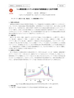
9 The process provides elec-troforming of uniform low stress gold deposit. The SU-8resist has low X-ray absorption and good radiation stability(Simon et ); this allows leaving resist in placewithout losing the mask contrast. A photograph and anoptical microscope image of one of the fabricated masksare shown in The grid area is 60960 mm, septawidth is 25lm, periodicity is 300lm, and the thickness ofgold absorber is 1 Photograph and close-up image (insert) of the mask for gridfabrication1614 Microsyst Technol (2008) 14:1613 Resist and substrate preparation: PMMA versus SU-8We use both a positive polymethylmethacrylate (PMMA,Goodfellow, CQ-grade), and a negative SU-8 (Micro-Chem) tone photoresists for the mold Fabrication for metalelectroforming.
10 PMMA process is well established, reliable and allowsfabrication of very high-aspect-ratio structures withhigh fidelity (Khan Malek et ,2003; Pantenburget ). We have fabricated grid structures up to3 mm tall (aspect ratio over 100) using deep X-raylithography and copper electroforming (Makarova et ,2003,2004a,b,c). The use of PMMA requires X-rays from the synchrotron. Unfortunately, beam linesare not readily available for many researchers, andrelatively long exposure times make the processexpensive. SU-8 negative resist developed by IBM with its highsensitivity to X-rays and excellent resolution is a newcheaper alternative to PMMA. The use of SU-8 insteadof PMMA significantly reduces the cost of the fabri-cation process because of much shorter X-ray exposuretime.