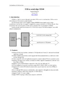
Transcription of FQP30N06L 60V LOGIC N-Channel MOSFET
1 May 2001 QFETTMFQP30N06L 2001 Fairchild Semiconductor CorporationRev. A1. May 2001 FQP30N06L60V LOGIC N-Channel MOSFETG eneral DescriptionThese N-Channel enhancement mode power field effecttransistors are produced using Fairchild s proprietary,planar stripe, DMOS advanced technology has been especially tailored tominimize on-state resistance, provide superior switchingperformance, and withstand high energy pulse in theavalanche and commutation mode. These devices are wellsuited for low voltage applications such as automotive, DC/DC converters, and high efficiency switching for powermanagement in portable and battery operated 32A, 60V, RDS(on) = @VGS = 10 V Low gate charge ( typical 15 nC) Low Crss ( typical 50 pF) Fast switching 100% avalanche tested Improved dv/dt capability 175 C maximum junction temperature ratingAbsolute Maximum Ratings TC = 25 C unless otherwise notedThermal Characteristics SymbolParameterFQP30N06 LUnitsVDSSD rain-Source Voltage60 VIDD rain Current - Continuous (TC = 25 C)
2 32A- Continuous (TC = 100 C) Current - Pulsed(Note 1)128 AVGSSGate-Source Voltage 20 VEASS ingle Pulsed Avalanche Energy(Note 2)350mJIARA valanche Current(Note 1)32 AEARR epetitive Avalanche Energy(Note 1) Diode Recovery dv/dt(Note 3) Dissipation (TC = 25 C)79W- Derate above 25 CTJ, TSTGO perating and Storage Temperature Range-55 to +175 CTLM aximum lead temperature for soldering purposes,1/8" from case for 5 seconds300 CSymbolParameterTypMaxUnitsR JCThermal Resistance, C/WR CSThermal Resistance, C/WR JAThermal Resistance, C/W!"!!!"""!"!!!"""SDG TO-220 FQP SeriesGSDFQP30N06 LRev. A1. May 2001 2001 Fairchild Semiconductor CorporationElectrical Characteristics TC = 25 C unless otherwise notedNotes:1.
3 Repetitive Rating : Pulse width limited by maximum junction temperature2. L = 400 H, IAS = 32A, VDD = 25V, RG = 25 , Starting TJ = 25 C3. ISD 32A, di/dt 300A/us, VDD BVDSS, Starting TJ = 25 C 4. Pulse Test : Pulse width 300us, Duty cycle 2%5. Essentially independent of operating temperatureSymbolParameterTest ConditionsMinTypMaxUnitsOff CharacteristicsBVDSSD rain-Source Breakdown Voltage VGS = 0 V, ID = 250 A60----V BVDSS/ TJBreakdown Voltage Temperature Coefficient ID = 250 A, Referenced to 25 CIDSSZero Gate Voltage Drain CurrentVDS = 60 V, VGS = 0 V----1 AVDS = 48 V, TC = 150 C----10 AIGSSFGate-Body Leakage Current, ForwardVGS = 20 V, VDS = 0 V ----100nAIGSSRGate-Body Leakage Current, ReverseVGS = -20 V, VDS = 0 V -----100nAOn Characteristics VGS(th)Gate Threshold Voltage VDS = VGS, ID = 250 (on)
4 Static Drain-Source On-ResistanceVGS = 10 V, ID = 16 AVGS = 5 V, ID =16 A gFSForward TransconductanceVDS = 25 V, ID = 16 A --24--SDynamic CharacteristicsCissInput CapacitanceVDS = 25 V, VGS = 0 V, f = MHz --8001040pFCossOutput Capacitance--270350pFCrssReverse Transfer Capacitance--5065pFSwitching Characteristics td(on)Turn-On Delay TimeVDD = 30 V, ID = 16 A,RG = 25 --1540nstrTurn-On Rise Time--210430nstd(off)Turn-Off Delay Time--60130nstfTurn-Off Fall Time--110230nsQgTotal Gate ChargeVDS = 48 V, ID = 32 A,VGS = 5 V --1520nCQgsGate-Source Diode Characteristics and Maximum RatingsISMaximum Continuous Drain-Source Diode Forward Current----32 AISMM aximum Pulsed Drain-Source Diode Forward Current----128 AVSDD rain-Source Diode Forward VoltageVGS = 0 V, IS = 32 A Recovery TimeVGS = 0 V, IS = 32 A,dIF / dt = 100 A/ s --60--nsQrrReverse Recovery Charge--90--nC (Note 4) (Note 4, 5) (Note 4, 5) (Note 4)
5 FQP30N06L 2001 Fairchild Semiconductor CorporationRev. A1. May 2001051015202530024681012 VDS = 30 VVDS = 48V Not e : ID = 32A VGS, Gate-Source Voltage [V]QG, Total Gate Charge [nC]10-11001010500100015002000 Ciss = Cgs + Cgd (Cds = shorted)Coss = Cds + CgdCrss = Cgd Notes : 1. VGS = 0 V 2. f = 1 MHzCrssCossCiss Capacitance [pF]VDS, Drain-Source Voltage [V] C Notes : 1. VGS = 0V 2. 250 s Pulse Test25 C IDR, Reverse Drain Current [A]VSD, Source-Drain voltage [V]0 20406080100120020406080 VGS = 10 VVGS = 5V Note : TJ = 25 C RDS(ON) [m ],Drain-Source On-ResistanceID, Drain Current [A]0246810100101102175 C25 C-55 C Notes : 1.
6 VDS = 25V 2. 250 s Pulse Test ID, Drain Current [A]VGS, Gate-Source Voltage [V]Typical CharacteristicsFigure 5. Capacitance CharacteristicsFigure 6. Gate Charge CharacteristicsFigure 3. On-Resistance Variation Current and Gate VoltageFigure 4. Body Diode Forward Voltage Variation vs. Source Current and TemperatureFigure 2. Transfer CharacteristicsFigure 1. On-Region Characteristics10-1100101100101102 VGSTop : V V V V V V VBottom : V Notes : 1. 250 s Pulse Test 2.
7 TC = 25 C ID, Drain Current [A]VDS, Drain-Source Voltage [V] FQP30N06L 2001 Fairchild Semiconductor CorporationRev. A1. May 200110-510-410-310-210-110010110-210-110 0 Notes : 1 . Z JC(t) = 0 C/W M a x . 2 . D u t y F a c t o r , D = t1/t2 3 . TJM - TC = PDM * Z JC(t)single pulseD= Z JC(t), Therm al R esponset1, S q u a re W a v e P u ls e D u ra tio n [s e c ]255075100125150175010203040 ID, Drain Current [A]TC, Case Temperature [ C]10-1100101102100101102 DC10 ms1 ms100 sOperation in This Area is Limited by R DS(on) Not es : 1. TC = 25 oC 2. TJ = 175 oC 3. Single Pulse ID, Drain Current [A]VDS, Drain-Source Voltage [V] Notes : 1.
8 VGS = 10 V 2. ID = 16 A RDS(ON), (Normalized)Drain-Source On-ResistanceTJ, Junction Temperature [oC] Notes : 1. VGS = 0 V 2. ID = 250 A BVDSS, (Normalized)Drain-Source Breakdown VoltageTJ, Junction Temperature [oC]Typical Characteristics (Continued)Figure 9. Maximum Safe Operating AreaFigure 10. Maximum Drain Currentvs. Case TemperatureFigure 7. Breakdown Voltage Variationvs. TemperatureFigure 8. On-Resistance Variationvs. TemperatureFigure 11. Transient Thermal Response Curvet1 PDMt2 FQP30N06L 2001 Fairchild Semiconductor CorporationRev. A1. May 2001 Gate Charge Test Circuit & Waveform Resistive Switching Test Circuit & Waveforms Unclamped Inductive Switching Test Circuit & WaveformsChargeVGS5 VQgQgsQgd3mAVGSDUTVDS300nF50K 200nF12 VSame Typeas DUTC hargeVGS5 VQgQgsQgd3mAVGSDUTVDS300nF50K 200nF12 VSame Typeas DUTVGSVDS10%90%td(on)trtontofftd(off)tfV DD5 VVDSRLDUTRGVGSVGSVDS10%90%td(on)trtontof ftd(off)tfVDD5 VVDSRLDUTRGVGSEAS =LIAS2----21--------------------BVDSS-VD DBVDSSVDDVDSBVDSSt pVDDIASVDS (t)ID (t)Time10 VDUTRGLIDt pEAS =LIAS2----21 EAS =LIAS2----21----21--------------------BV DSS-VDDBVDSSVDDVDSBVDSSt pVDDIASVDS (t)ID (t)
9 Time10 VDUTRGLLIDIDt pFQP30N06L 2001 Fairchild Semiconductor CorporationRev. A1. May 2001 Peak Diode Recovery dv/dt Test Circuit & WaveformsDUTVDS+_DriverRGSame Type as DUTVGS dv/dt controlled by RG ISDcontrolled by pulse period VDDLISD10 VVGS( Driver )ISD( DUT )VDS( DUT )VDDBody DiodeForward Voltage DropVSDIFM, Body Diode Forward CurrentBody Diode Reverse CurrentIRMBody Diode Recovery dv/dtdi/dtD =Gate Pulse WidthGate Pulse Period--------------------------DUTVDS+_ DriverRGSame Type as DUTVGS dv/dt controlled by RG ISDcontrolled by pulse period VDDLLISD10 VVGS( Driver )ISD( DUT )VDS( DUT )VDDBody DiodeForward Voltage DropVSDIFM, Body Diode Forward CurrentBody Diode Reverse CurrentIRMBody Diode Recovery dv/dtdi/dtD =Gate Pulse WidthGate Pulse Period--------------------------D =Gate Pulse WidthGate Pulse Period--------------------------FQP30N06 L 2001 Fairchild Semiconductor CorporationRev.
10 A1. May 2001 Package ( ) ( )( )( )( )( )(45 ) + + [ ] [ ]TO-220 2001 Fairchild Semiconductor CorporationRev. H2 TRADEMARKSThe following are registered and unregistered trademarks Fairchild Semiconductor owns or is authorized to use and is notintended to be an exhaustive list of all such SEMICONDUCTOR RESERVES THE RIGHT TO MAKE CHANGES WITHOUT FURTHER NOTICE TO ANYPRODUCTS HEREIN TO IMPROVE RELIABILITY, FUNCTION OR DESIGN. FAIRCHILD DOES NOT ASSUME ANYLIABILITY ARISING OUT OF THE APPLICATION OR USE OF ANY PRODUCT OR CIRCUIT DESCRIBED HEREIN;NEITHER DOES IT CONVEY ANY LICENSE UNDER ITS PATENT RIGHTS, NOR THE RIGHTS OF SUPPORT POLICYFAIRCHILD S PRODUCTS ARE NOT AUTHORIZED FOR USE AS CRITICAL COMPONENTS IN LIFE SUPPORTDEVICES OR SYSTEMS WITHOUT THE EXPRESS WRITTEN APPROVAL OF FAIRCHILD used herein:1.