Transcription of Fully Integrated Dickson Charge Pumps with Optimized …
1 Abstract This paper describes how the power efficiency of Fully Integrated Dickson Charge Pumps in advanced smart power technologies can be improved considerably by implementing Charge recycling techniques and the replacement of normal PN junction diodes by pulse-driven active diodes. These 2 methods are first analyzed and compared on a purely theoretical basis and are verified with experimental data afterwards. Measurements reveal that the combination of the 2 methods can boost the power efficiency by a factor of 2 compared to traditional Dickson Charge pump designs. Index Terms Charge recycling, Dickson Charge pump, high-voltage generator, power efficiency optimization, smart power technology. I. INTRODUCTION Fully Integrated Charge Pumps are used in a wide variety of applications, going from flash memories to dedicated display drivers.
2 Some applications ask for specific features, such as high current drive capability or a very good output voltage stability, but for all of them a good overall power efficiency is of the utmost importance. Achieving high power efficiency in Fully Integrated Dickson Charge Pumps is not straightforward due to the fact that Integrated capacitors exhibit considerable parasitic capacitance to the substrate, resulting in a dramatic efficiency drop. In this paper Charge recycling techniques are presented to substantially reduce this negative effect. Replacing the standard PN junction diodes by pulse-driven DMOS transistors acting as almost ideal active diodes is another method to enhance the power efficiency. In this paper, both methods are described theoretically and verified experimentally.
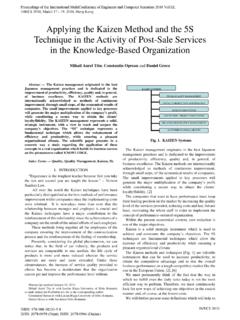
3 II. BASIC Dickson Charge PUMP DESIGN The basic configuration of a Dickson Charge pump [1] is shown in Fig. 1. It consists of a large number of identical stages, each containing a diode and a capacitor, where the bottom plates of the capacitors in consecutive stages are driven by 2 complementary clock signals. Charge is transferred from one capacitor to the next at the rhythm of the clock, yielding an output voltage that can be much higher Manuscript received July 5, 2010. Jan Doutreloigne is with the Centre for Microsystems Technology (CMST), affiliated to the Interuniversity Microelectronics Centre (IMEC) and the University of Gent, Technologiepark 914A, 9052 Zwijnaarde, Belgium (phone: +32-(0)9-264-53-56; fax: +32-(0)9-264-53-74; e-mail: than the input voltage. In a real application, a feedback control loop is added to the circuit in order to maintain the output voltage very stable and independent of system parameters or load characteristics.)
4 This can be achieved by continuously adjusting the clock frequency of the Charge pump. FIGURE 1. BASIC Dickson Charge PUMP. Writing down the Charge balance in each capacitor under steady-state circumstances yields the following simple expression for the output voltage Vout as a function of the output current Iout, the number of stages n, the clock frequency f and the capacitor value C: ([2], [3], [4]) CfoutIngVnoutV )1( The quantity Vg is the voltage gain per stage under zero-load conditions and is given by: TVccVgV where Vcc represents the supply voltage of the Charge pump and VT the forward voltage drop or threshold voltage of a diode. We will now illustrate the design of such a Charge pump for a specific situation. Let's assume that the Charge pump must be capable of boosting a 3V supply voltage up to 60V output voltage under zero-load conditions.
5 For a diode threshold voltage, the previous equations indicate that 23 stages are needed to reach this goal. If we further assume that the application requires that the output voltage is still at least 50V at 50 A output current at a maximum clock frequency Fully Integrated Dickson Charge Pumps with Optimized Power Efficiency Jan Doutreloigne Proceedings of the World Congress on Engineering and Computer Science 2010 Vol II WCECS 2010, October 20-22, 2010, San Francisco, USAISBN: 978-988-18210-0-3 ISSN: 2078-0958 (Print); ISSN: 2078-0966 (Online)WCECS 2010 of 10 MHz, the same equations yield a minimum 12pF capacitor in each stage. The question now is which type of Integrated capacitor we best choose. In fact, each so-called smart power technology, which is actually a high-voltage extension to a standard CMOS core process, offers several types of Integrated capacitors to the chip designers.
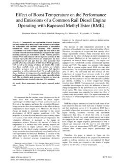
6 The choice of 1 particular capacitor type does not only depend on the specific capacitance per unit silicon area and the maximum operating voltage, but also on the parasitic capacitance between the bottom plate of the capacitor and the substrate of the chip, as illustrated in Fig. 2: FIGURE 2. PRESENCE OF PARASITIC CAPACITANCE. The parasitic capacitance Cp does not contribute to the useful operation of the circuit, but it does affect the power consumption in a negative way. Indeed, the parasitic capacitance Cp is connected directly to the output of the clock buffers, and these buffers have to Charge and discharge this parasitic capacitance constantly, resulting in additional power losses inside the transistors of the clock buffers, without having any useful impact on the circuit operation. Hence, the lower the value of this parasitic capacitance, the better the power efficiency will be.
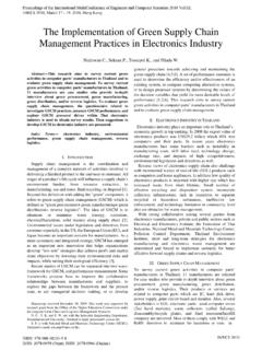
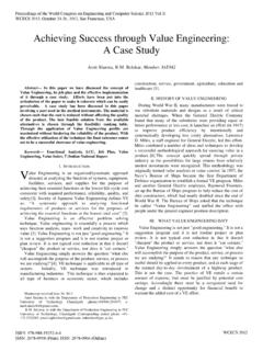
7 In order to illustrate what types of capacitors are available in an advanced smart power technology, we ll consider the specific example of the 100V m I2T technology (Intelligent Interface Technology) of ON Semiconductor. Figs. 3 to 5 show a vertical cross section of 3 different kinds of Integrated capacitors in this technology. Fig. 3 depicts a capacitor between a poly-silicon layer at the top and a highly doped N+ implantation at the bottom, with a very thin dielectric in between. Fig. 4 represents a capacitor structure between 2 poly-silicon layers, with a somewhat thicker dielectric. Finally, Fig. 5 shows a sandwich structure where the shorted poly-silicon and metal2 layers form 2 capacitors in parallel towards the metal1 layer. The dielectric in this structure is considerably thicker than in the 2 previous cases.
8 FIGURE 3. POLY-N+ CAPACITOR (PN CAPACITOR). FIGURE 4. POLY1-POLY2 CAPACITOR (PP CAPACITOR). FIGURE 5. METAL1-METAL2-POLY CAPACITOR (MM CAPACITOR). Depending on the thickness of the dielectric, these capacitor types have different values of the specific capacitance per unit silicon area and maximum operating voltage, but also the parasitic capacitance towards the substrate behaves differently. These data are gathered in Table I. Apparently, the PN capacitor has the highest specific capacitance per unit silicon area because of the thinnest dielectric, but at the same time also the lowest maximum operating voltage. At the other extreme, the MM capacitor has the highest maximum operating voltage at the expense of the lowest specific capacitance per unit silicon area. The PP capacitor is settled somewhere in between.
9 Regarding the parasitic capacitance towards the substrate, the PP capacitor is undoubtedly the best option, and the MM capacitor clearly the worst. Capacitor type Max. voltage (V) Specific capacitance (fF/ m2) Parasitic capacitance (fF/ m2) PN 12 0,75 0,27 (36%) PP 30 0,345 0,079 (23%) MM 100 0,091 0,057 (63%) TABLE I. COMPARISON OF DIFFERENT CAPACITOR TYPES. Based on the information from Table I we can easily select the most appropriate capacitor type for every individual stage in the Dickson Charge pump. The most important selection criterion is of course the maximum operating voltage. In the first 4 stages, where the capacitor operating voltage is limited to values below 12V, the PN capacitor type is definitely the best choice because of the highest specific capacitance per unit silicon area, resulting in the most cost-effective solution.
10 Proceedings of the World Congress on Engineering and Computer Science 2010 Vol II WCECS 2010, October 20-22, 2010, San Francisco, USAISBN: 978-988-18210-0-3 ISSN: 2078-0958 (Print); ISSN: 2078-0966 (Online)WCECS 2010 In the next 8 stages, where the operating voltage is within the range from 12V to 30V, the PP capacitor is selected. Finally, for the 11 last stages with operating voltages in excess of 30V, the MM capacitor is the only remaining option. The very bad corresponding parasitic capacitance towards the substrate is something we have to live with ! In order to assess the power efficiency of the Charge pump, we first have to calculate the average current delivered by the supply voltage Vcc. This average supply current is given by the following expression: ccVCfnoutIntotinI )1(, The first term represents the average current the clock buffers have to supply to the bottom plates of the capacitors in each stage in order to compensate the Charge loss caused by the output current drawn by the load.