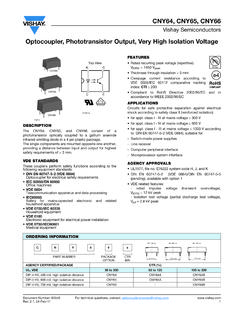
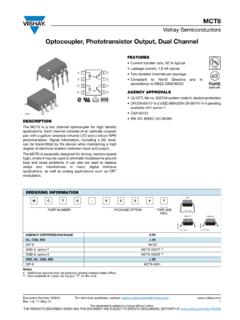
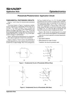
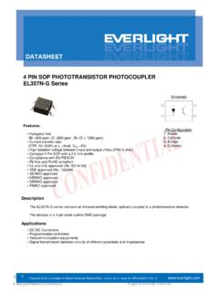
Transcription of H22A1 H22A2 H22A3 Phototransistor Optical …
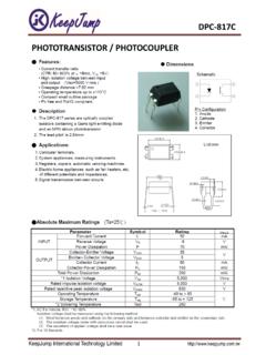
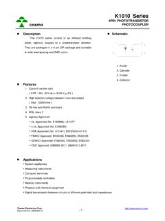
1 H22A1 H22A2 H22A3 Phototransistor Optical Interupter Switch Light in Motion LLC TR/LiM10/003 17/09/10 Page 1 of 4 H22A1 H22A2 H22A3 Phototransistor Optical Interrupter Switch Features No Contact Sensing 1mm Aperture High IC(ON) PCB mount Transistor output Description The H22AX products consist of a infrared light emitting diode coupled to an NPN silicon Phototransistor pack-aged in a injection molded housing. The package is designed to optimize the mechanical resolution, cou-pling efficiency, ambient light rejection, and reliability. Inserting/removing an opaque material into the gap when the LED is operating, switches the transistor on/off. Package Dimensions Notes 1. Dimensions for all drawings are in millimeters. 2. Tolerance of +/- on all non nominal dimensions unless otherwise specified Schematic Pin 1 Anode Pin 2 Cathode Pin 3 Collector Pin 4 Emitter H22A1 H22A2 H22A3 Phototransistor Optical Interrupter Switch Light in Motion LLC TR/LiM10/003 17/09/10 Page 2 of 4 Absolute Maximum Ratings (TA = 25O C unless otherwise specified) Stresses exceeding the absolute maximum ratings may damage the device.
2 The device may not function or be operable above the recommended operating conditions and stressing the parts to these levels is not recommended. In Addition, extended exposure to stresses above the recommended operating conditions may affect device reliability. The absolute maximum ratings are stress ratings only. Notes: 1. Derate power dissipation linearly mW/OC above 25OC. 2. Derate power dissipation linearly mW/OC above 25OC. 3. RMA Flux is recommended. 4. Methanol or isopropyl alcohols are recommended as cleaning agents. 5. Soldering iron tip from housing. 6. As long as leads are not under stress or spring tension Electrical/ Optical Characteristics (TA = 25O C ) Symbol Parameter Rating Units TOPR Operating Temperature -55 to +100 OC TSTG Storage Temperature -55 to +100 OC TSOL-I Soldering Temperature (Iron) (3,4,5) 240 for 5 sec OC TSOL-F Soldering Temperature (Flow) (3,4) 260 for 10 sec OC Emitter IF Continuous Forward Current (6) 60 mA VR Reverse Voltage 6 V PD Power Dissipation (1) 100 mW Sensor VCEO Collector-Emitter Voltage 30 V VECO Emitter-Collector Voltage V PD Power Dissipation (2) 150 mW EMITTER Symbol Parameter Test Conditions Min.
3 Typ. Max. Units VF Forward Voltage IF = 60mA V VR Reverse Breakdown Voltage IR = 10 A 6 V SENSOR Symbol Parameter Test Conditions Min. Typ. Max. Units BVCEO Collector-Emitter Breakdown Voltage IC = 1mA, Ee = 0 30 V BVECO Emitter-Collector Breakdown Voltage IEC = 100uA, Ee = 0 6 V ICEO Collector-Emitter Leakage VCE = 25V, Ee = 0 100 nA H22A1 H22A2 H22A3 Phototransistor Optical Interrupter Switch Light in Motion LLC TR/LiM10/003 17/09/10 Page 3 of 4 Electrical/ Optical Characteristics Cont. (TA = 25O C ) COUPLED Symbol Parameter Test Conditions Min.
4 Typ. Max. Units t(ON) Turn-on Time IF = 30mA, VCC = 5V, RL = 8 s t(OFF) Turn-Off Time IF = 30mA, VCC = 5V, RL = 50 s ON-STATE COLLECTOR CURRENT Symbol Device Test Conditions Min. Typ. Max. Units IC (ON) H22A1 IF = 5mA, VCE = 5V mA H22A2 H22A3 H22A1 IF = 20mA, VCE = 5V mA H22A2 H22A3 H22A1 IF = 30mA.
5 VCE = 5V mA H22A2 3 H22A3 COLLECTOR CURRENT SATURATION VOLTAGE Symbol Device Test Conditions Min. Typ. Max. Units VCE (SAT) H22A1 , H22A2 , H22A3 , IC = , IF = 20mA V V Typical Performance Characteristics H22A1 H22A2 H22A3 Phototransistor Optical Interrupter Switch Light in Motion LLC TR/LiM10/003 17/09/10 Page 4 of 4 Typical Performance Characteristics DISCLAIMER LIGHT IN MOTION LLC RESERVES THE RIGHT TO MAKE CHANGES WITHOUT FURTHER NOTICE TO ANY PRODUCTS HEREIN TO IMPROVE RELIABILITY.
6 FUNCTION OR DESIGN. LIGHT IN MOTION DOES NOT ASSUME ANY LIABILITY ARISING OUT OF THE APPLICATION OR USE OF ANY PRODUCT OR CIRCUIT DESCRIBED HEREIN; NEITHER DOES IT CONVEY ANY LICENSE UNDER ITS PATENT RIGHTS, NOR THE RIGHTS OF OTHERS. LIFE SUPPORT POLICY LIGHT IN MOTION S PRODUCTS ARE NOT AUTHORIZED FOR USE AS CRITICAL COMPONENTS IN LIFE SUPPORT DEVICES OR SYSTEMS WITHOUT THE EXPRESS WRITTEN APPROVAL OF THE PRESIDENT OF LIGHT IN MOTION LLC. As used herein: 1. Life support devices or systems are devices or systems 2. A critical component in any component of a life support which, (a) are intended for surgical implant into the body, device or system whose failure to perform can be or (b) support or sustain life, and (c) whose failure to reasonably expected to cause the failure of the life support perform when properly used in accordance with device or system, or to affect its safety or effectiveness. instructions for use provided in the labeling, can be reasonably expected to result in a significant injury of the user.
7