Transcription of High Frequency 50 GHz Thin Film Chip Resistor
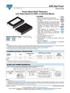
1 Sfernice Revision: 22-Jul-20201 Document Number: 53014 For technical questions, contact: DOCUMENT IS SUBJECT TO CHANGE WITHOUT NOTICE. THE PRODUCTS DESCRIBED HEREIN AND THIS DOCUMENTARE SUBJECT TO SPECIFIC DISCLAIMERS, SET FORTH AT Frequency 50 GHz thin film chip ResistorLINKS TO ADDITIONAL RESOURCEST hose miniaturized components are designed in such a way that their internal reactance is very small. When correctly mounted and utilized, they function as almost pure resistors on a very large range of Frequency , up to 50 Operating Frequency 50 GHz thin film microwave resistors Flip chip , wraparound or one face termination Small size, down to 20 mils by 16 mils Edged trimmed block resistors Pure alumina substrate ( %) Ohmic range: 10R to 500R Design kits available Small internal reactance (LC down to 1 x 10-24) Tolerance 1 %, 2 %, 5 % TCR: 100 ppm/ C in (-55 C, +155 C) temperature range TCR: 50 ppm/ C available upon request for 10 to150 ohmic range Material categorization.
2 For definitions of compliance please see (1) ( )333 DDD3D3D ModelsS-ParametersSTANDARD ELECTRICAL SPECIFICATIONSMODELSIZERESISTANCE RANGE RATED POWERPnWLIMITING ELEMENTVOLTAGEVTOLERANCE %TEMPERATURECOEFFICIENT ppm/ CCH020160201610 to , 5100 (50 upon request)CH0402040210 to , 2, 5100 (50 upon request)CH0603060310 to , 2, 5100 (50 upon request)DIMENSIONS in millimeters (inches)CH02016 F / CH02016 P /CH0402 P / CH0603 PCH0402 F / CH0603 FCH0402 N / CH0402 G /CH0603 N / CH0603 GCASE SIZE MODEL / TERMINATIONDIMENSIONSA ( )B ( )C ( )DE when applicableF ( )G ( ) F CH02016 ( ) ( ) ( ) (1) ( ) ( ) ( ) ( )CH0402 F CH0402 N CH0402 ( ) ( ) ( ) ( ) ( )n/an/aCH0402 ( ) ( ) ( ) ( ) ( ) ( ) ( )CH0603 F CH0603 N CH0603 ( ) ( ) ( ) ( ) ( )n/an/aCH0603 ( ) ( ) ( ) ( ) ( ) ( ) ( ) Sfernice Revision: 22-Jul-20202 Document Number: 53014 For technical questions, contact: DOCUMENT IS SUBJECT TO CHANGE WITHOUT NOTICE.
3 THE PRODUCTS DESCRIBED HEREIN AND THIS DOCUMENTARE SUBJECT TO SPECIFIC DISCLAIMERS, SET FORTH AT Suggested land pattern: According to IPC-7351 Dimension and tolerance of land pattern shall be defined by PCB designer; PCB can be designed according to IPC-7351A Generic Requirements for Surface Mount Design and Land Pattern Standard TOLERANCE VS. OHMIC VALUESO hmic range10 R < 50 50 R 500 Tolerance CH020165 %2 %, 5 %Tolerance CH0402 and CH06032 %, 5 %1 %, 2 %, 5 %LAND PATTERN FOR F 'FLIP chip ' TERMINATIONS in millimeters (inches) chip ( ) ( ) ( ) ( ) ( ) ( ) ( ) ( ) ( )LAND PATTERN FOR N AND G WRAPAROUND TERMINATIONS in millimeters (inches) chip ( ) ( ) ( ) ( ) ( ) ( ) Sfernice Revision: 22-Jul-20203 Document Number: 53014 For technical questions, contact: DOCUMENT IS SUBJECT TO CHANGE WITHOUT NOTICE. THE PRODUCTS DESCRIBED HEREIN AND THIS DOCUMENTARE SUBJECT TO SPECIFIC DISCLAIMERS, SET FORTH AT MODELS AND VALUESV ishay Sfernice highly recommend to use the smallest sizes and flip chip version to get the best Values:10R/18R/25R/50R/75R/100R/150R/180 R/200R/250R/330R/500R Those values are available with a MOQ of 100 pieces.
4 Other values can be ordered upon request, but higher MOQ will apply: 1000 pieces for CH02016, 500 pieces for CH0402, 250 pieces for termination:FRecommended tolerance:2 %DESIGN KITSD esign kits are available Ex Stock in CH02016 and CH0402 sizes. There are 20 pieces per recommended value. F termination. 5 % tolerance. Those kits are packaged in pieces of tape and delivered in ESD packaging is plastic tape and reel for all sizes. Paper tape and reel is available for sizes 0402 and 0603. Waffle pack is available for all on the type of terminations, parts will be packed differently:One face: Gold terminations:(P termination option):active face up Tin / silver terminations: (F termination option):active face down in tape and reel active face up in waffle packNote Please refer to vishay Sfernice Application Note Guidelines for vishay Sfernice Resistive and Inductive Products for soldering recommendation (document number 52029, 3.)
5 Guidelines for Surface Mounting Components (SMD), profile number 3 appliesPACKAGING RULESW affle PackCan be filled up to maximum quantity indicated in the table here above, taking into account the minimum order quantity. When quantity ordered exceeds maximum quantity of a single waffle pack, the waffle packs are stacked up on the top of each other and closed by one single cover. To get not stacked up waffle pack in case of ordered quantity > maximum number of pieces per package: Please consult vishay Sfernice for specific ordering and ReelSee Part Numbering information to get the quantity desired by regard to the CH02016 size only, up to 5 empty cavities can be found every 1000 parts in the reel. Nevertheless, the number of requested parts will be respected. SIZEMOQNUMBER OF PIECES PER PACKAGETAPE WIDTHWAFFLE PACK2" x 2"TAPE AND MOQ mentioned on preferred models and values48410050008 Sfernice Revision: 22-Jul-20204 Document Number: 53014 For technical questions, contact: DOCUMENT IS SUBJECT TO CHANGE WITHOUT NOTICE.
6 THE PRODUCTS DESCRIBED HEREIN AND THIS DOCUMENTARE SUBJECT TO SPECIFIC DISCLAIMERS, SET FORTH AT Historical part numbers are not recommended but can still be used for ordering(1)Gold termination for application in hermetic package. Can also be mounted on PCB with SnAg solder paste(2)CHKIT for 0603 size is not availableGLOBAL PART NUMBER INFORMATIONNew Global Part Numbering: CH0402-50 RJF (preferred part number format)GLOBAL MODELSIZEOHMIC VALUETOLERANCETERMINATIONPACKAGINGOPTION CH020160402060310R to 500RF = 1 %G = 2 %J = 5 %F (flip chip ):SnAg over nickel barrierN (W/A):SnAg over nickel barrier(except 02016)P (one face): (1)gold bonding padsG (W/A): gold over nickel barrier(except 02016)For moreinformation see Codification of Packaging tableFrom1 to 3 blankif no Part Number example: CH02016-100 RGFPT1K (tapes of 1K pieces) CH0402-50 RJF(waffle pack)CHKIT Part Numbers (2):CHKIT-02016 CHKIT-0402 CODIFICATION OF PACKAGINGWAFFLE PACK (available for all sizes)W100 min.
7 , 1 TAPE (standard packaging for all sizes)T100 min., 1 min., 100 min., 250 min., 500 min., 1000 min., 2500 tape (quantity depending on size of chips)PAPER TAPE (available for 0402 and 0603)PT100 min., 1 min., 100 min., 250 min., 500 (not available for size 0402)1000 min., 1000 (not available for size 0402)2500 min., 2500 (not available for size 0402)Full tape (quantity depending on size of chips)TYPICAL high Frequency PERFORMANCE ELECTRICAL MODELCI nternal shunt capacitanceLInternal inductanceRResistanceZInternal impedance (R, L, C)LcExternal connection inductanceCgExternal capacitance to groundLcCgZ0 CLRZZ0 LcCgH04 02 - Sfernice Revision: 22-Jul-20205 Document Number: 53014 For technical questions, contact: DOCUMENT IS SUBJECT TO CHANGE WITHOUT NOTICE. THE PRODUCTS DESCRIBED HEREIN AND THIS DOCUMENTARE SUBJECT TO SPECIFIC DISCLAIMERS, SET FORTH AT complex impedance of the chip Resistor is given by the following equations:Notes = 2 x x f f: frequencyR, L and C are relevant to the chip Resistor itself.
8 Lc and Cg also depend on the way the chip Resistor is mounted. It is important to notice that after assembly the external reactance of Lc and Cg will be combined to internal reactance of L and C. This combination can upgrade or downgrade the HF behavior of the component. This is why we are displaying three sets of data: versus Frequency curves which aim to show at a glance the intrinsic HF performance of a given chip Resistor versus Frequency curves which aim to show the behavior of the chip Resistor when mountedThese lines are terminated with adapted source and load impedance respectively Zs and Zl with Z0 = ZL = Zs (for others configurations please consult us).Equivalent circuit for S-parameters:S-parameters are computed taking into account all the resistive, inductive and capacitive elements (Z total) and Z0 = ZL = Zs = simulation purposes, those S-parameter data are available for download here: j L R2C L2C 2 ()+1CR2C 2L () 2 L2C 4+[]+----------------------------------- ---------------------------------------- -----------=Z[]R--------11 CR2C 2L () 2 L2C 4+[]+----------------------------------- ---------------------------------------- --------------- x 1 L R2C L2C 2 ()R------------------------------------- -----------------------2+= tan1 L R2C L2C 2 ()R------------------------------------- -----------------------=Z[]R--------Ztot al[]R-------------------LcCgZ0 CLRZ Sfernice Revision: 22-Jul-20206 Document Number: 53014 For technical questions, contact: DOCUMENT IS SUBJECT TO CHANGE WITHOUT NOTICE.
9 THE PRODUCTS DESCRIBED HEREIN AND THIS DOCUMENTARE SUBJECT TO SPECIFIC DISCLAIMERS, SET FORTH AT IMPEDANCE (GHz) Internal impedance curve for 02016 size (F and P terminations)10 50 75 100 150 200 250 500 (GHz) Internal impedance curve for 0402 size (F and P terminations)10 50 75 100 150 200 250 500 Sfernice Revision: 22-Jul-20207 Document Number: 53014 For technical questions, contact: DOCUMENT IS SUBJECT TO CHANGE WITHOUT NOTICE. THE PRODUCTS DESCRIBED HEREIN AND THIS DOCUMENTARE SUBJECT TO SPECIFIC DISCLAIMERS, SET FORTH AT IMPEDANCE (GHz) Internal impedance curve for 0402 size (N and G terminations)10 75 100 150 200 250 500 50 (GHz) Internal impedance curve for 0603 size (F and P terminations)10 50 75 100 150 200 250 500 Sfernice Revision: 22-Jul-20208 Document Number: 53014 For technical questions, contact: DOCUMENT IS SUBJECT TO CHANGE WITHOUT NOTICE.
10 THE PRODUCTS DESCRIBED HEREIN AND THIS DOCUMENTARE SUBJECT TO SPECIFIC DISCLAIMERS, SET FORTH AT IMPEDANCE CURVESINTERNAL IMPEDANCE CURVES (|ZTOTAL| / R) (GHz) Internal impedance curve for 0603 size (N and G terminations)10 50 75 100 150 200 250 500 (GHz) Internal impedance curve for 02016 size (F and P terminations)25 100 200 250 500 50 75 150 Sfernice Revision: 22-Jul-20209 Document Number: 53014 For technical questions, contact: DOCUMENT IS SUBJECT TO CHANGE WITHOUT NOTICE. THE PRODUCTS DESCRIBED HEREIN AND THIS DOCUMENTARE SUBJECT TO SPECIFIC DISCLAIMERS, SET FORTH AT IMPEDANCE CURVES (|ZTOTAL| / R) (GHz) impedance curve for 0402 size (F and P terminations)10 25 50 200 250 500 75 150 100 (GHz) impedance curve for 0402 size (N and G terminations)10 25 50 200 250 500 75 150 100 Sfernice Revision: 22-Jul-202010 Document Number: 53014 For technical questions, contact: DOCUMENT IS SUBJECT TO CHANGE WITHOUT NOTICE.
