Transcription of High Temperature (245 °C) Thick Film Chip Resistor
1 Sfernice Revision: 24-Jan-181 Document Number: 52032 For technical questions, contact: DOCUMENT IS SUBJECT TO CHANGE WITHOUT NOTICE. THE PRODUCTS DESCRIBED HEREIN AND THIS DOCUMENTARE SUBJECT TO SPECIFIC DISCLAIMERS, SET FORTH AT Temperature (245 C) Thick film chip ResistorDESIGN SUPPORT TOOLSFEATURES high Temperature (245 C) Large ohmic value range to 100 M Operating Temperature range (-55 C to +230 C) SMD wraparound chip Resistor Storage Temperature range (-55 C to +245 C) Gold terminations for HMP process (< 1 m Thick ) for Temperature up to 245 C Tin / silver terminations for operating Temperature up to 200 C Material categorization.
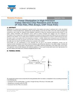
2 For definitions of compliance please see applications such as down hole applications or aircraft breaking systems, the need for parts able to withstand very severe conditions ( Temperature as high as 230 C powered or up to 245 C un-powered) has leaded vishay Sfernice to push out the limit of the Thick film technology. Designers might read the application note Power Dissipation Considerations in high Precision vishay Sfernice Thin film Chips Resistors and Arrays (P, PRA etc.) ( high Temperature Applications) ( ) in conjunction with this data sheet to help them to properly design their PCBs and get the best performances of the CHPHT.
3 vishay Sfernice R&D engineers will be willing to support any customer design logo to get startedAvailableModelsAvailableDIMENSION S in millimetersCASE SIZEABCDE LAND PATTERN (to IPC-7351A)CASE Sfernice Revision: 24-Jan-182 Document Number: 52032 For technical questions, contact: DOCUMENT IS SUBJECT TO CHANGE WITHOUT NOTICE. THE PRODUCTS DESCRIBED HEREIN AND THIS DOCUMENTARE SUBJECT TO SPECIFIC DISCLAIMERS, SET FORTH AT Refer to Application Note Guidelines for vishay Sfernice Resistive and Inductive Components (document number: 52029) for recommended reflow profile. Profile #3 appliesPOWER DERATING CURVEPACKAGINGESD packaging available: Waffle pack and plastic tape and reel (low conductivity).
4 Paper tapes available on request (ESD only). (For 0603, 0805, and 1206 only.)PACKAGING RULESW affle Pack Can be filled up to maximum quantity indicated in the table here above, taking into account the minimum order quantity. When quantity ordered exceeds maximum quantity of a single waffle pack, the waffle packs are stacked up on the top of each other and closed by one single cover. To get not stacked up waffle pack in case of ordered quantity > maximum number of pieces per package: Please consult vishay Sfernice for specific ordering codeTape and Reel Can be filled up to maximum quantity indicated in the table here above, taking into account the minimum order quantity.
5 When quantity ordered is between the MOQ and the maximum reel capacity, only one reel is provided. When several reels are needed for ordered quantity within MOQ and maximum reel capacity: Please consult vishay Sfernice for specific ordering codeSTANDARD ELECTRICAL SPECIFICATIONSMODELSIZERESISTANCE RANGE RATED POWERPnW(at 230 C)LIMITING ELEMENT VOLTAGE VOLTAGE VTOLERANCE % Temperature COEFFICIENT ppm/ to , 2, 5100, to , 2, 5100, to , 2, 5100, to , 2, 5100, 200 CLIMATIC SPECIFICATIONSO perating Temperature range-55 C to +230 CStorage Temperature range-55 C to +245 CMECHANICAL SPECIFICATIONSS ubstrateAluminaTechnologyThick film (Ruthenium oxyde) < R < 100 M :double organic coatingR.
6 Overglaze protection (no organic coating)TerminationsN (W/A): SnAg over nickel barrier for temperatureup to 200 CG (W/A) type: Gold (< 1 m) over nickel barrier for temperatureup to 245 CBEST TOL. AND TCR VERSUS OHMIC VALUETIGHTEST TOLERANCEOHMICVALUESBEST TCRppm/ C1 % (F)5 < R < 10M100 (K)2 % (G)1 < R < R (L)5 % (J) < R < R (L)Ambient Temperature in CRated Power (%)1200100080060040020005020010030001502 50 SIZENUMBER OF PIECESPER PACKAGETAPEWIDTHWAFFLEPACKTAPE AND Sfernice Revision: 24-Jan-183 Document Number: 52032 For technical questions, contact: DOCUMENT IS SUBJECT TO CHANGE WITHOUT NOTICE. THE PRODUCTS DESCRIBED HEREIN AND THIS DOCUMENTARE SUBJECT TO SPECIFIC DISCLAIMERS, SET FORTH AT OPTIONSFor any option it is recommended to consult vishay Sfernice for availability : Enlarged terminations: For stringent and special power dissipation requirements, the thermal resistance between the resistive layer and the solder joint can be reduced using enlarged terminations chip resistors which are soldered on large and Thick copper pads acting as heat sinks (see application note: Power Dissipation in high Precision vishay Sfernice chip Resistors and Arrays (P Thin film , PRA Arrays, CHP Thick film ( ).))
7 Option to order: 0063 (applies to size 1206/2010).DIMENSIONS (Option 0063) in millimetersSUGGESTED LAND PATTERN (Option 0063)CASE SIZEABEDFMAX. TOL.+ TOL.+ TOL.+ TOL.+ ( ) ( ) ( ) ( ) ( ) ( ) ( ) ( ) ( ) ( ) ( ) ( ) ( ) ( ) chip SIZEDIMENSIONS (in millimeters) ( ) ( ) ( ) ( ) ( ) ( )ABDEFE nlargedterminationUncoatedceramicBottom view for Sfernice Revision: 24-Jan-184 Document Number: 52032 For technical questions, contact: DOCUMENT IS SUBJECT TO CHANGE WITHOUT NOTICE. THE PRODUCTS DESCRIBED HEREIN AND THIS DOCUMENTARE SUBJECT TO SPECIFIC DISCLAIMERS, SET FORTH AT (1)N terminations for Temperature up to 200 C G terminations for Temperature up to 230 C PERFORMANCETESTSCONDITIONSREQUIREMENTSTY PICAL VALUESAND DRIFTST ermination adhesion5N for 10 s ( % + )< %Resistance to solder heatImmersion 10 s in Sn/Pb 60/40 at +260 C ( % + )< %Rapid Temperature change5 cycles-55 C to +155 C ( % + )< %Climatic sequencePhase A dry heatPhase B damp heatPhase C cold -55 CPhase D damp heat 5 cycles (1 % + )< %Humidity (steady state)56 days (1 % + )
8 < %Moisture resistanceAEC-Q20085 C / 85 % RH / Pn1000 h3 % + Max. < 3 % + Short time Pnfor 2 s ( % + )< %Load life1000 h at rated power at 230 C-1 % life1000 h at 245 C-1 % PART NUMBER INFORMATIONG lobal Part Numbering: CHPHT0805K1001 FGTGLOBALMODELSIZETCRVALUETOLERANCETERMINATION (1)PACKAGINGOPTIONCHPHT0603080512062010K = 100 ppmL = 200 ppmThe first 3 digitsare significantfigures and thelast digit specifiesthe number of zeros to designatesdecimal point10R0 = 10 3901 = 3900 1004 = 1 M F = 1 %G = 2 %J = 5 %N: SnAg over nickel barrierG: gold over nickel barrierFor more information see Codification of packaging tableLeave blankif no optionHPHT0805KC10 0 Sfernice Revision.
9 24-Jan-185 Document Number: 52032 For technical questions, contact: DOCUMENT IS SUBJECT TO CHANGE WITHOUT NOTICE. THE PRODUCTS DESCRIBED HEREIN AND THIS DOCUMENTARE SUBJECT TO SPECIFIC DISCLAIMERS, SET FORTH AT OF PACKAGINGWAFFLE PACKW100 min., 1 multWA100 min., 100 mult (available only in size 1206)PLASTIC TAPE (Standard for all sizes)T100 min., 1 multTA100 min., 100 multTB250 min., 250 multTC500 min., 500 multTD1000 min., 1000 multTE2500min., 2500 multTFFull tape (quantity depending on size of chips)PAPER TAPE (Available for 0603, 0805, and 1206. Please consult vishay Sfernice for other sizes)PT100 min., 1 multPA100 min., 100 multPB250 min., 250 multPC500 min.
10 , 500 multPD1000 min., 1000 multPE2500min., 2500 multPFFull tape (quantity depending on size of chips)CODIFICATION OF OPTIONS ON TWO DIGITSOPTIONOPTION 2 DIGITSOPTIONOPTION 2 OF SIZESCODE 18 CODE 40 CODE 18 CODE 40702016M2280302N3390402O44A0502P55B0505 Q515C0603R48D0805S408E1005T816F1010U914G 1020V073H1206W074I1505X100J2010Y135K2208 Z182L2512 Legal Disclaimer Revision: 08-Feb-171 Document Number: 91000 Disclaimer ALL PRODUCT, PRODUCT SPECIFICATIONS AND DATA ARE SUBJECT TO CHANGE WITHOUT NOTICE TO IMPROVE RELIABILITY, FUNCTION OR DESIGN OR OTHERWISE. vishay Intertechnology, Inc., its affiliates, agents, and employees, and all persons acting on its or their behalf (collectively, vishay ), disclaim any and all liability for any errors, inaccuracies or incompleteness contained in any datasheet or in any other disclosure relating to any makes no warranty, representation or guarantee regarding the suitability of the products for any particular purpose or the continuing production of any product.
