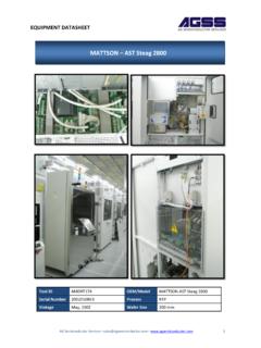
Transcription of Hitachi S-9300 CD SEM - AG Semiconductor
1 Hitachi S- 9300 CD SEM. Manufacturer: Hitachi Model: S- 9300 . Wafer Size: 200mm Electron Optical System Electron Gun: Schottky emission source Accelerating voltage: 500V to 1600V, 10V steps Probe Current: 4~24pA with automated setting and measurement by Faraday cup Electromagnetic Lens: 3 Stage Electromagnetic Lens System with boosting voltage Objective Lens: 4 opening click stop, heated aperture is selectable/adjustable outside the vacuum Scan Coil: 2-Stage Electromagnetic Deflection Astigmatism correction via an 8-pole electromagnetic coil Magnification = 1000x to >300000x Field control method ; Continuously on for sample decharging, at all voltages Wafer imaging ability; Entire surface of 8 (or 12 ) wafer Depth of focus: >= at 80000x magnification Resolution: 3nm (800V) Retarding/Boosting Mode Hitachi Probe Tip Optical Microscope System Image is Monochrome, using CCD camera Magnification is 110x Wafer imaging: X coverage from 5 295mm, Y coverage from 5 195mm , notch down Field of View: Workstation Model: HP B180L (9GB).
2 O/S: Unix version HP-UX or newer Software version: or newer SECS/GEM Communication Interface Dual XY Hitachi Microscale DSP Image Processing BSE Mode Functionality Multipoint Measurement Function Edge Roughness Function Automated Image Archiving Function Other 200mm Wafer Handling System: (2) Cassette holders/ergo flippers Convertible to 300mm with conversion kit BRK-287006300. Edwards ESDP30 Pump, vib iso and vertinlet/exhaust (subject to availability). Water Chiller Unit (subject to availability). Additional details available upon request NOTE: The information has been prepared for your convenience by AG Semiconductor Services, Inc. (AGSS). While we have endeavored to keep the information up-to-date, we make no representations or warranties of any kind about the completeness, accuracy or reliability of this information including, without limitation, the availability for sale, the accuracy or completeness of the description of any such item or any picture thereof, the price or condition of any such item, or the suitability of any such item for any purpose.
3 Any reliance you place on this information is strictly and completely at your own risk. Our liability in all cases shall be limited to what is expressly set forth in written sale agreements duly signed and delivered by the purchaser of equipment and an authorized officer of AGSS.


