Transcription of Integrated Video Decoder and Dual Mode HDMI/MHL …
1 Integrated Video Decoder and dual Mode HDMI/MHL Receiver Data Sheet ADV7481 FEATURES Analog input Worldwide ntsc /PAL/SECAM color demodulation support with autodetection One 10-bit ADC, 4 oversampling for CVBS, Y/C, and YPbPr 8 analog Video input channels with on-chip antialiasing filter Fully differential, pseudo differential, and single-ended CVBS Video input support STB diagnostics on differential Video inputs CVBS (composite), Y/C (S- Video ), and YPbPr (component) Video input support Fast switching capability between analog inputs Adaptive contrast enhancement (ACE) Excellent common-mode noise rejection capabilities Rovi (Macrovision) copy protection detection Up to 4 V common-mode input range solution Vertical blanking interval (VBI) data slicer Mobile High-Definition Link (MHL) capable receiver High-bandwidth Digital Content Protection (HDCP) authentication and decryption support 75 MHz maximum pixel clock frequency, allowing HDTV formats up to 720p/1080i at 60 Hz 24 bits per pixel mode supported HDCP repeater support, up to 25 KSVs supported Adaptive TMDS equalizer High-Definition Multimedia Interface (HDMI) capable receiver HDCP authentication and decryption support 162 MHz maximum pixel clock frequency, allowing HDTV formats up to 1080p and display resolutions up to UXGA (1600 1200 at 60 Hz) HDCP repeater support, up to 25 KSVs supported Integrated CEC controller, CEC compatible Adaptive TMDS equalizer 5 V detect and Hot Plug assert Component Video processor Any-to-any 3 3 color space conversion (CSC) matrix Contrast/brightness/hue/saturation Video adjustment Timing adjustments controls for horizontal sync (HS)/vertical sync (VS)/data enable (DE)
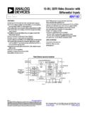
2 Timing Video mute function Serial digital audio output interface HDMI/MHL audio extraction support Advanced audio muting feature I2S-compatible, left justified, and right justified audio output modes 8-channel TDM output mode available 2 Mobile Industry Processor Interface (MIPI) Camera Serial Interface 2 (CSI-2) transmitters 4-lane transmitter with 4 lanes, 2 lanes, and 1 lane muxing options for HDMI/MHL /SDP/digital input port sources 1-lane transmitter for standard definition processor (SDP) sources 8-bit digital input/output port General 2-wire serial microprocessor unit (MPU) interface (I2C compatible) 40 C to +85 C temperature grade 100-ball, 9 mm 9 mm, RoHS-compliant CSP_BGA package Qualified for automotive applications APPLICATIONS Portable devices Automotive infotainment (head unit and rear seat entertainment systems) HDMI repeaters and Video switches FUNCTIONAL BLOCK DIAGRAM Figure 1. RX0P/RX0 NRX1P/RX1 NRX2P/RX2 NRXCP/RXCNDDC_SCL/CD_PULLUPDDC_SDAHPD/CB USRX_5V/VBUSVBUS_ENCD_SENSECECHDMI/MHLRE CEIVERCPCOREAUDIOPROCESSORSPI SLAVEI2C SLAVEINTERRUPTSCONTROLLERAUDIO OUTPUTFORMATTERSPI_MISOSPI_MOSISPI_SCLKS PI_CSDIAGNOSTIC8-BIT TTLINPUT/OUTPUTAFECECHPDEDID RAMHDCPMHL_SENSECBUSDDCSCLKSDATAALSBINTR Q1 TOINTRQ3I2S_MCLKI2S_LRCLKI2S_SCLKI2S_SDA TACLKAP/CLKANCLKBP/CLKBNDB0P/DB0 NAIN1 TOAIN8P0TO P7 LLCDIAG1 TODIAG4DA0P/DA0 NTODA3P/DA3N4-LANEMIPI CSI-2 TRANSMITTER1-LANEMIPI CSI-2 TRANSMITTERADV7481 SDCORE12046-001 Rev.
3 0 Document Feedback Information furnished by Analog Devices is believed to be accurate and reliable. However, no responsibility is assumed by Analog Devices for its use, nor for any infringements of patents or other rights of third parties that may result from its use. Specifications subject to change without notice. No license is granted by implication or otherwise under any patent or patent rights of Analog Devices. Trademarks and registered trademarks are the property of their respective owners. One Technology Way, Box 9106, Norwood, MA 02062-9106, Tel: 2014 Analog Devices, Inc. All rights reserved. Technical Support ADV7481 Data Sheet TABLE OF CONTENTS Features .. 1 Applications .. 1 Functional Block Diagram .. 1 Revision History .. 2 General Description .. 3 Detailed Functional Block Diagram .. 4 Specifications .. 5 Electrical Characteristics .. 5 Analog Video Specifications .. 7 MIPI Video Output Specifications.
4 8 Analog Specifications .. 8 Timing Specifications .. 9 Absolute Maximum Ratings .. 13 Thermal Resistance .. 13 ESD Caution .. 13 Pin Configuration and Function Descriptions .. 14 Power Supply Recommendation .. 17 Power-Up Sequence .. 17 Power-Down Sequence .. 17 Theory of Operation .. 18 Combined HDMI/MHL Receiver .. 18 MHL Receiver .. 18 HDMI Receiver .. 18 Component Processor .. 19 Analog Front End .. 19 Short to Battery Diagnostics .. 19 Standard Definition Processor .. 20 8-Bit Digital Input/Output Port .. 20 Audio Processing .. 21 MIPI CSI-2 Transmitters .. 21 Interrupts .. 21 Outline Dimensions .. 22 Ordering Guide .. 22 Automotive Products .. 22 REVISION HISTORY 6/14 Revision 0: Initial Version Rev. 0 | Page 2 of 22 Data Sheet ADV7481 GENERAL DESCRIPTION The ADV7481 is an Integrated Video Decoder and combined HDMI /MHL receiver. It is targeted at connectivity enabled head units requiring a wired, uncompressed digital audio/ Video link from smartphones and other consumer electronics devices to support streaming and integration of cloud-based multimedia content and applications into an automotive infotainment system.
5 The ADV7481 MHL capable receiver supports a maximum pixel clock frequency of 75 MHz, allowing resolutions up to 720p/1080i at 60 Hz in 24-bit mode. The ADV7481 features a link control bus (CBUS) that handles the link layer, translation layer, CBUS electrical discovery, and display data channel (DDC) commands. The implementation of the MHL sideband channel (MSC) commands by the system processor can be handled either by the I2C bus, or via a dedicated serial peripheral interface (SPI) bus. A dedicated interrupt pin (INTRQ3) is available to indicate that events related to CBUS have occurred. The ADV7481 also features an enable pin (VBUS_EN) to dynamically enable or disable the output of a voltage regulator, which provides a 5 V voltage bus (VBUS) signal to the MHL source. The ADV7481 HDMI capable receiver supports a maximum pixel clock frequency of 162 MHz, allowing HDTV formats up to 1080p, and display resolutions up to UXGA (1600 1200 at 60 Hz). The device integrates a consumer electronics control (CEC) controller that supports the capability discovery and control (CDC) feature.
6 The HDMI input port has dedicated 5 V detect and Hot Plug assert pins. The HDMI/MHL receiver includes an adaptive transition minimized differential signaling (TMDS) equalizer that ensures robust operation of the interface with long cables. The ADV7481 single receiver port is capable of accepting both HDMI and MHL electrical signals. Automatic detection between HDMI and MHL is achieved by using cable impedance detection through the CD_SENSE pin. The ADV7481 contains a component processor (CP) that processes the Video signals from the HDMI/MHL receiver. It provides features such as contrast, brightness, and saturation adjustments, as well as free run and timing adjustment controls for HS/VS/DE timing. The ADV7481 analog front end (AFE) comprises a single high speed, 10-bit analog-to -digital converter (ADC) that digitizes the analog Video signal before applying it to the SDP. The eight analog Video inputs can accept single-ended, pseudo differential, and fully differential composite Video signals, as well as S- Video and YPbPr Video signals, supporting a wide range of consumer and automotive Video sources.
7 Short to battery (STB) events can be detected on differential input Video signals. STB protection is provided by ac coupling the input Video signals. The ADV7481, in combination with an external resistor divider, provides a common-mode input range of 4 V, enabling the removal of large signal common-mode transients present on the Video lines. The automatic gain control (AGC) and clamp restore circuitry allow an input Video signal up to V p-p at the analog Video input pins of the ADV7481. Alternatively, the AGC and clamp restore circuitry can be bypassed for manual settings. The SDP of the ADV7481 is capable of decoding a large selection of analog baseband Video signals in composite, S- Video , and component formats. The SDP supports world-wide ntsc , PAL, and SECAM standards. The ADV7481 features an 8-bit digital input/output port, supporting input and output Video resolutions up to 720p/1080i in both the 8-bit interleaved 4:2 :2 SDR and DDR modes. To enable glueless interfacing of these Video input sources to the latest generation of infotainment system on chips (SoCs) , the ADV7481 features two MIPI CSI-2 transmitters.
8 The four-lane transmitter provides four data lanes, two data lanes, and one data lane muxing options, and can be used to output Video from the HDMI receiver, the MHL receiver, the SDP, and the digital input port. The single-lane transmitter can be used to output Video from the SDP only. The ADV7481 offers a flexible audio output port for audio data extracted from the MHL or HDMI streams. The HDMI/MHL receiver has advanced audio functionalit y, such as a mute controller that prevents audible extraneous noise in the audio output. Additionally, the ADV7481 can be set to output time division multiplexing (TDM) serial audio, which allows the transmission of eight multiplexed serial audio channels on a single audio output interface port. The ADV7481 is programmed via a 2-wire, serial, bidirectional port (I2C compatible). Fabricated in an advanced CMOS process, the ADV7481 is available in a 9 mm 9 mm, RoHS-compliant, 100-ball CSP_BGA package and is specified over the 40 C to +85 C temperature range.
9 The ADV7481 is offered in automotive and industrial versions. Rev. 0 | Page 3 of 22 ADV7481 Data Sheet DETAILED FUNCTIONAL BLOCK DIAGRAM Figure 2. INTRQ1 INTRQ2 INTRQ3I2S_MCLKI2S_LRCLKI2S_SCLKI2S_SDATA CLKAP/CLKANDA0P/DA0 NDA1P/DA1 NDA2P/DA2 NDA3P/DA3 NADV7481 GENERALINTERRUPTSCONTROLLERI2C SLAVE/CONTROLSCLKSDATAALSBRESETSPISLAVES PI_MISOMIPI CSI-2 TRANSMITTER AAUDIO OUTPUTFORMATTERRX0P/RX0 NRX1P/RX1 NRX2P/RX2 NRXCP/RXCNVBUS_ENCBUSCONTROLLERMHL LINKDISCOVERYBLOCK5V DETECTANDHPD PINCONTROLLERCECCONTROLLEREQUALIZEROUTPU T BLOCK FIFOPLLEDID/REPEATERCONTROLLER8-BITDIGIT ALINPUT/OUTPUTPORTLLCSAMPLERHDCPENGINEHD CPKEYSHDMI/MHLPROCESSORCOMPONENTPROCESSO R(CP)PACKETPROCESSORAUDIOPROCESSORPACKET /INFOFRAMEMEMORYCBUSINTERRUPTSCONTROLLER 8-BITTO6-BITDITHERBLOCKACEDOWN-DITHERCOL ORSPACECONVERSIONCSI-2 TxD-PHY TxCLKBP/CLKBNDB0P/DB0 NMIPI CSI-2 TRANSMITTER BVREFPVREFNCSI-2 TxD-PHY TxSPI_MOSISPI_SCLKSPI_CSDDC_SDADDC_SCL/C D_PULLUPCD_SENSEHPD/CBUSRX_5V/VBUSCECP0P 1P2P3P4P5P6P7 DIAGNOSTICSCLOCK PROCESSING BLOCKPLLADLLT PROCESSINGREFERENCEAIN7 AIN8 AFEMUX BLOCK+ SHAADC10-BITADCAAFILTERAAFILTERAAFILTERA AFILTERXTALPXTALNSTANDARD DEFINITIONPROCESSOR (SDP)2D COMBVBI SLICERCOLOR DEMODSTANDARDAUTODETECTIONDIAG1 DIAG2 DIAG3 DIAG4 AIN5 AIN6 AIN3 AIN4 AIN1 AIN212046-002 Rev.
10 0 | Page 4 of 22 Data Sheet ADV7481 SPECIFICATIONS ELECTRICAL CHARACTERISTICS AVDD = V to V, DVDD = V to V, PVDD = V to V, MVDD = V to V, CVDD = V to V, DVDDIO = V to V, and TVDD = V to V, specified at operating temperature range, unless otherwise noted. Table 1. Parameter Symbol Test Conditions/Comments Min Typ Max Unit STATIC PERFORMANCE Resolution (Each ADC) N 10 Bits Integral Nonlinearity INL CVBS mode 2 LSB Differential Nonlinearity DNL CVBS mode LSB DIGITAL INPUTS1 SCLK, SDATA, RESET, ALSB, SPI_CS, SPI_SCLK, SPI_MOSI, LLC, and P0 to P7 Input High Voltage VIH DVDDIO = V to V 2 V Input Low Voltage VIL DVDDIO = V to V V Input Leakage Current IIN 10 +10 A Input Capacitance2 CIN 10 pF CRYSTAL INPUT Input High Voltage VIH XTALP V Input Low Voltage VIL XTALP V DIGITAL OUTPUTS1 LLC, P0 to P7, I2S_MCLK, I2S_SCLK, I2S_LRCLK, I2S_SDATA, SPI_MISO, SDATA, INTRQ1 to INTRQ3 (when configured to drive when active)