Transcription of Introduction to Digital Design Using Digilent FPGA Boards
1 Introduction to Digital Design Using Digilent FPGA Boards Block Diagram / VHDL Examples richard e . haskell Darrin M. Hanna Oakland University, Rochester, Michigan LBE Books Rochester Hills, MI ii Copyright 2009 by LBE Books, LLC. All rights reserved. ISBN 978-0-9801337-6-9 Online Version Published by LBE Books, LLC 1202 Walton Boulevard Suite 214 Rochester Hills, MI 48307 iii Preface A major revolution in Digital Design has taken place over the past decade. Field programmable gate arrays (FPGAs) can now contain over a million equivalent logic gates and tens of thousands of flip-flops. This means that it is not possible to use traditional methods of logic Design involving the drawing of logic diagrams when the Digital circuit may contain thousands of gates. The reality is that today Digital systems are designed by writing software in the form of hardware description languages (HDLs).
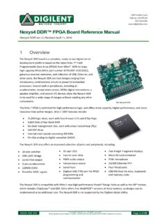
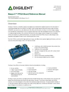
2 The most common HDLs used today are VHDL and Verilog. Both are in widespread use. When Using these hardware description languages the designer typically describes the behavior of the logic circuit rather than writing traditional Boolean logic equations. Computer-aided Design tools are used to both simulate the VHDL or Verilog Design and to synthesize the Design to actual hardware. This book assumes no previous knowledge of Digital Design . We use 30 examples to show you how to get started designing Digital circuits that you can implement on a Xilinx Spartan3E FPGA Using either the Digilent BASYS system board that can be purchased from for $59 or the Digilent Nexys-2 board that costs $99. We will use Active-HDL from Aldec to Design , simulate, synthesize, and implement our Digital designs. A free student edition of Active-HDL is available from Aldec, Inc.
3 ( ). To synthesize your designs to a Spartan3E FPGA you will need to download the free ISE WebPACK from Xilinx, Inc. ( ). The Xilinx synthesis tools are called from within the Aldec Active-HDL integrated GUI. We will use the ExPort utility to download your synthesized Design to the Spartan3E FPGA. ExPort is part of the Adept software suite that you can download free from Digilent , Inc. ( ). A more complete book called Digital Design Using Digilent FPGA Boards VHDL / Active-HDL Edition is also available from Digilent or LBE Books ( ). This more comprehensive book contains over 75 examples including examples of Using the VGA and PS/2 ports. Similar books that use Verilog are also available from Digilent or LBE Books. Many colleagues and students have influenced the development of this book. Their stimulating discussions, probing questions, and critical comments are greatly appreciated.
4 richard e . haskell Darrin M. Hanna iv Introduction to Digital Design Using Digilent FPGA Boards Block Diagram / VHDL Examples Table of Contents Introduction Digital Design Using FPGAs 1 Example 1 Switches and LEDs 6 Example 2 2-Input Gates 11 Example 3 Multiple-Input Gates 16 Example 4 Equality Detector 21 Example 5 2-to-1 Multiplexer 23 Example 6 Quad 2-to-1 Multiplexer 27 Example 7 4-to-1 Multiplexer 34 Example 8 Clocks and Counters 42 Example 9 7-Segment Decoder 48 Example 10 7-Segment Displays: x7seg and x7segb 54 Example 11 2's Complement 4-Bit Saturator 64 Example 12 Full Adder 70 Example 13 4-Bit Adder 75 Example 14 N-Bit Adder 79 Example 15 N-Bit Comparator 82 Example 16 Edge-Triggered D Flip-Flop Available only in print vesion Example 17 D Flip-Flops in VHDL Example 18 Divide-by-2 Counter Example 19 Registers Example 20 N-Bit Register in VHDL Example 21 Shift Registers
5 Example 22 Ring Counters Example 23 Johnson Counters Example 24 Debounce Pushbuttons Example 25 Clock Pulse Example 26 Arbitrary Waveform Example 27 Pulse-Width Modulation (PWM) Example 28 Controlling the Position of a Servo Example 29 Scrolling the 7-Segment Display Example 30 Fibonacci Sequence vAppendix A Aldec Active-HDL Tutorial 123 Part 1: Project Setup 123 Part 2: Design Entry 127 Part 3: Synthesis and Implementation 130 Part 4: Program FPGA Board 134 Part 5: Design Entry 136 Part 6: Simulation 142 Part 7.
6 Design Entry HDE 146 Part 8: Simulation gates2 149 Appendix B Number Systems Available only in print vesion Counting in Binary and Hexadecimal Positional Notation Fractional Numbers Number System Conversions Negative Numbers Appendix C Basic Logic Gates Truth Tables and Logic Equations
7 Positive and Negative Logic: De Morgan s Theorem Sum of Products Design Product of Sums Design Appendix D Boolean Algebra and Logic Equations Boolean Theorems Karnaugh Maps Appendix E VHDL Quick Reference Guide 189
8 Introduction 1 Introduction Digital Design Using FPGAs The first integrated circuits that were developed in the early 1960s contained less that 100 transistors on a chip and are called small-scale integrated (SSI) circuits. Medium-scale integrated (MSI) circuits, developed in the late 1960s, contain up to several hundreds of transistors on a chip. By the mid 1970s large-scale integrated (LSI) circuits containing several thousands of transistors had been developed. Very-large-scale integrated (VLSI) circuits containing over 100,000 transistors had been developed by the early 1980s. This trend has continued to the present day with 1,000,000 transistors on a chip by the late 1980s, 10,000,000 transistors on a chip by the mid-1990s, over 100,000,000 transistors by 2004, and up to 1,000,000,000 transistors on a chip today.
9 This exponential growth in the amount of Digital logic that can be packed into a single chip has produced serious problems for the Digital designer. How can an engineer, or even a team of engineers, Design a Digital logic circuit that will end up containing millions of transistors? In Appendix C we show that any Digital logic circuit can be made from only three types of basic gates: AND, OR, and NOT. In fact, we will see that any Digital logic circuit can be made Using only NAND gates (or only NOR gates), where each NAND or NOR gate contains four transistors. These basic gates were provided in SSI chips Using various technologies, the most popular being transistor-transistor logic (TTL). These TTL chips were the mainstay of Digital Design throughout the 1960s and 1970s. Many MSI TTL chips became available for performing all types of Digital logic functions such as decoders, adders, multiplexers, comparators, and many others.
10 By the 1980s thousands of gates could fit on a single chip. Thus, several different varieties of programmable logic devices (PLDs) were developed in which arrays containing large numbers of AND, OR, and NOT gates were arranged in a single chip without any predetermined function. Rather, the designer could Design any type of Digital circuit and implement it by connecting the internal gates in a particular way. This is usually done by opening up fuse links within the chip Using computer-aided tools. Eventually the equivalent of many PLDs on a single chip led to complex programmable logic devices (CPLDs). Field Programmable Gate Arrays (FPGAs) A completely different architecture was introduced in the mid-1980 s that uses RAM-based lookup tables instead of AND-OR gates to implement combinational logic. These devices are called field programmable gate arrays (FPGAs). The device consists of an array of configurable logic blocks (CLBs) surrounded by an array of I/O blocks.
