Transcription of Ion implantation in silicon technology - Axcelis.com
1 12 The Industrial Physicist Ion implanters are essential to modern integrated-cir-cuit (IC) manufacturing. Doping or otherwise modify-ing silicon and other semiconductor wafers relies on thetechnology, which involves generating anion beam and steering it into the sub-strate so that the ions come to restbeneath the surface. Ions may be allowedto travel through a beam line at the ener-gy at which they were extracted from asource material, or they can be accelerat-ed or decelerated by dc or radio-frequen-cy (RF) electric processors today useion implantation for almost all doping in silicon ICs. Themost commonly implanted species are arsenic, phospho-rus, boron, boron difluoride, indium, antimony, germa-nium, silicon , nitrogen, hydrogen, and helium. Implant-ing goes back to the 19th century, and has been continu-ally refined ever since.
2 Physicist Robert Van de Graaff ofthe Massachusetts Institute of technology and PrincetonUniversity helped pioneer accelerator construction, andthe high-voltage technology that emerged from this effortwas instrumental in building High Voltage EngineeringCorp. (HVEC) in the late 1940s and 1950s. HVEC served as an incubator for the technology essential tobuilding the first commercial ion implanters and theindividuals who pioneered the Shockley first recognized the potential of ionimplantation for doping semiconductor materials, andhis 1954 patent application demonstrates a remarkableunderstanding of the relevant process issues long beforeimplantation entered mass production. However, thepatent expired in 1974, just as the commercial ion- implantation market began taking off. So althoughShockley demonstrated visionary insight, hispatent earned few equipment and applica-tions gradually came together in the gained in building researchaccelerators improved hardware reliabilityand generated new techniques for purifyingand transporting ion beams.
3 Theoristsrefined the hypothesis of ion stopping,which enabled the precise placement of ionsbased on the energy and angle of implanta-tion, and experimenters determined thathigh-temperature postimplant annealingcould repair implantation -induced crystaldamage. Initially, these anneals were done ata temperature of 500 to 700 C, but afterseveral years, semiconductor processorsfound that the optimum annealing tempera-ture ranged from 900 to 1,100 C. After theresolution of process integration issues, ionimplantation rapidly displaced thermal dif-fusion of deposited dopants as the dominantmethod of semiconductor doping because itwas more precise, reliable, and manufacturers, especially IBM andWestern Electric, designed and built many ofthe early ion implanters, almost exclusivelyfor in-house use.
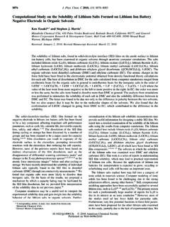
4 But in the early 1970s, themarket for commercial ion implanters beganopening as start-up companies tapped thetechnology spun off from HVEC and theIon implantation inSilicon Technologyby Leonard Rubin and John PoateFEATUREJUNE/JULY 2003 American Institute of PhysicsWithoutimplanters,today s integratedcircuits would beimpossibleCONCENTRATION (atoms/cm3)DEPTH ( m)4 keV1 MeV2 MeV3 MeV012341021102010191018101710161015 Figure 1. Some of the most commonly implanted species highlightedon the periodic table, along with typical concentration-versus-depthtraces for various implant energies. technology developed by IC manufacturers, whobecame their customers. Some memory circuits now sell for less than 20nanodollars/transistor. Today, implanters and other fab-rication hardware must meet aggressive productivity tar-gets to achieve this minuscule cost.
5 A large wafer fabri-cator may process up to 50,000 wafers/month, witheach wafer requiring 20 to 30 implants. This outputrequires the use of about 20 implanters, each with thecapacity to implant more than 200 wafers/h. In practice,maximum implanter throughput typically ranges from250 to 270 wafers/h, including placing the wafers intoand removing them from sealed cassettes used by auto-mated material-handling systems. This throughput isachieved for wafer sizes of 150, 200, and 300 on the configuration of the beam line and theend station (the wafer-processing chamber), an implanteroccupies an area of 16 to 28 m2. Thus, fabrication spaceposes almost as significant a barrier as capital costagainst compensating for poor throughput by installingadditional Among semiconductor-processing techniques, ionimplantation is nearly unique in that process parameters,such as concentration and depth of the desired dopant,are specified directly in the equipment settings forimplant dose and energy, respectively (Figure 1).
6 This dif-fers from chemical vapor deposition, in which desiredparameters such as film thickness and densityare complex func-tions of the tun-able-equipmentsettings, whichinclude tempera-ture and gas-flowrate. The numberof implants need-ed to complete anIC has increasedas the complexityof the chips hasgrown. Whereasprocessing a sim-ple n-type metaloxide semiconduc-tor during the1970s may haverequired 6 to 8 implants, a modern complementary-metal-oxide-semiconductor (CMOS) IC with embeddedmemory may contain up to 35 technique s applications require doses and ener-gies spanning several orders of magnitude. Mostimplants fall within one of the boxes in Figure 2. Theboundaries of each box are approximate; individualprocesses vary because of differences in design trade-offs. Energy requirements for many applications havefallen with increased device scaling.
7 A shallower dopantprofile helps keep aspect ratios roughly constant as later-al device dimensions shrink. As energies drop, ion dosesusually, but not always, decline as well. The width of thestatistical distribution of the implanted ions decreaseswith energy, and this reduces the dose required to pro-duce a given peak dopant concentration. The result is13 The Industrial Physicist Bonded wafer splittingfor silicon on insulator(H, He) ,00010,000 ENERGY (keV)Polysilicondoping (As, B)Source draincontact(As, BF2, B)DOSE (atoms/cm2)Source drainextension(As, BF2, B) Preamorphization(Ge, Si) Bipolar buriedsubcollector (P, As)Latch-up/electrostatic dischargeprotection (B)CMOS retrogradewells(P, B, As)Channel engineering(As, BF2, P, B, In, Sb)Thresholdvoltage adjust(As, BF2, B, P, In)Antipunch-through(As, B, In, Sb)Noise isolationwells (P, B)Charge-coupleddevice wells (B)Dual-slit extractionelectrodeElectron confinementbeam guideAnalyzer magnet edge focusingElectron confinement beam tunnelFlag FaradaySelectableresolvinghousingDeceler ationgroundextentionPlasmaelectronflood( xenon)WaferFigure 2.
8 Dose andenergy require-ments of majorimplantation appli-cations (speciesshown roughly inorder of decreasingusage). Figure of theelectron confine-ment technologynecessary totransport severalmilliamperes ofbeam at energiesbelow 10 keV in amodern high-cur-rent beam The Industrial Physicist the sloping lines in Figure 2. implantation is actuallyextremely inefficient at modifying material highest ion dose implanted with an economicalthroughput is about 1016/cm2, yet this corresponds tobut 20 atomic layers. Only the extreme sensitivity ofsemiconductor conductivity to dopant concentrationmakes ion implantation energy requirements vary from less than 1 keV tomore than 3,000 keV. Accelerating ions to higher ener-gies requires a longer beam line, yet low-energy beamsare difficult to transport intact over longer distancesbecause the beam cross section expands to a point whereit can no longer travel down the beam tube.
9 This funda-mental physics makes it nearly impossible to construct abeam line capable of all required ion energies. Figure 2indicates that the largest magnitude in required dosesoccurs in the middle of the energy range. Because dose isessentially the beam s charge multiplied by the implanta-tion time, available beam currents in the 5- to 200-keVrange must vary by at least 4 orders of magnitude to per-form all required implants efficiently. This level is diffi-cult to reproduce repeatedly in a single ion-source/beam-line segmentsConsequently, the commercial ion-implanter marketlong ago evolved into three segments. The red, black,and blue regions of Figure 2 indicate high-current, medi-um-current, and high-energy applications, respectively. As the name suggests, high-current implantersproducethe highest beam currents, up to 25 mA (Figure 3).
10 Forhigh-dose applications, the greater the beam current, thefaster the implantation , which means the output of morewafers per hour. Implanter makers have invested a greatdeal of effort in maximizing beam current, especially at thelowest energies, where Child s law limits the flux of ionsextractable from a source. Although high-current implanterscan produce beams in the 10- A range, source instabilitiesmake these beams unsuitable for low-dose short beam line of these implanters allows an energyrange from <1 keV up to 100 to 200 implantersare designed for maxi-mum dose uniformity and beam currents are in the range of1 A to 5 mA, at energies of 5 to ~600 wafer-processing end stations canimplant ions at angles up to 60 from theperpendicular to the wafer surface. This isessential for certain applications, such asanti-punchthrough implants, for example,in which dopants must be implanted par-tially underneath a previously formed gatestructure.