Transcription of IRFF130 REPETITIVE AVALANCHE AND dv/dt RATED …
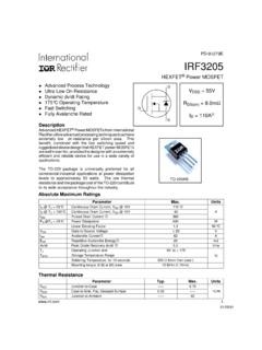
1 Features REPETITIVE AVALANCHE Ratings Dynamic dv/dt Rating Hermetically Sealed Simple Drive Requirements The HEXFET technology is the key to International Rectifier s HiRel advanced line of power MOSFET transistors. The efficient geometry and unique processing of this latest State of the Art design achieves: very low on state resistance combined with high trans conductance. The HEXFET transistors also feature all of the well established advantages of MOSFETs such as voltage control, very fast switching and temperature stability of the electrical parameters. They are well suited for applications such as switching power supplies, motor controls, inverters, choppers, audio amplifiers and high energy pulse circuits. Absolute Maximum Ratings Symbol Parameter Value Units ID1 @ VGS = 10V, TC = 25 C Continuous Drain Current A ID2 @ VGS = 10V.
2 TC = 100 C Continuous Drain Current IDM @ TC = 25 C Pulsed Drain Current 32 PD @ TC = 25 C Maximum Power Dissipation 25 W Linear Derating Factor W/ C VGS Gate-to-Source Voltage 20 V EAS Single Pulse AVALANCHE Energy 75 mJ IAR AVALANCHE Current A EAR REPETITIVE AVALANCHE Energy mJ dv/dt Peak Diode Recovery dv/dt V/ns TJ Operating Junction and C TSTG Storage Temperature Range Lead Temperature 300 ( in. mm from case for 10s) Weight (Typical) g -55 to + 150 TO-39 IRFF130 JANTX2N6796 JANTXV2N6796 1 2018-11-20 Product Summary Part Number BVDSS RDS(on) ID IRFF130 100V REPETITIVE AVALANCHE AND dv/dt RATED HEXFET TRANSISTORS THRU-HOLE TO-205AF (TO-39) PD-90430D Description For Footnotes, refer to the page 2.
3 International Rectifier HiRel Products, Inc. 100V, N-CHANNEL REF: MIL-PRF-19500/557 2 2018-11-20 IRFF130 JANTX2N6796/JANTXV2N6796 International Rectifier HiRel Products, Inc. Thermal Resistance Symbol Parameter Min. Typ. Max. Units R JC Junction-to-Case R JA Junction-to-Ambient (Typical Socket Mount) 175 C/W Electrical Characteristics @ Tj = 25 C (Unless Otherwise Specified) Symbol Parameter Min. Typ. Max. Units Test Conditions BVDSS Drain-to-Source Breakdown Voltage 100 V VGS = 0V, ID = BVDSS/ TJ Breakdown Voltage Temp.
4 Coefficient V/ C Reference to 25 C, ID = RDS(on) Static Drain-to-Source On-Resistance VGS = 10V, ID2 = VGS = 10V, ID1 = VGS(th) Gate Threshold Voltage V VDS = VGS, ID = 250 A Gfs Forward Transconductance S VDS = 15V, ID2 = IDSS Zero Gate Voltage Drain Current 25 A VDS =80 V, VGS = 0V 250 VDS = 80V,VGS = 0V,TJ =125 C IGSS Gate-to-Source Leakage Forward 100 nA VGS = 20V Gate-to-Source Leakage Reverse -100 VGS = -20V QG Total Gate Charge nC ID1 = QGS Gate-to-Source Charge VDS = 50V QGD Gate-to-Drain ( Miller ) Charge VGS = 10V td(on) Turn-On Delay Time 30 ns VDD = 50V tr Rise Time 75 ID1 = td(off) Turn-Off Delay Time 40 RG = tf Fall Time 45 VGS = 10V Ls +LD Total Inductance nH Measured from Drain lead (6mm / in from package) to Source lead (6mm/ in from package) with Source wire internally bonded from Source pin to Drain pin Ciss Input Capacitance 650 pF VGS = 0V Coss Output Capacitance 240 VDS = 25V Crss Reverse Transfer Capacitance 44 = Source-Drain Diode Ratings and Characteristics Symbol Parameter Min.
5 Typ. Max. Units Test Conditions IS Continuous Source Current (Body Diode) ISM Pulsed Source Current (Body Diode) 32 VSD Diode Forward Voltage V TJ = 25 C,IS = , VGS = 0V trr Reverse Recovery Time 300 ns TJ = 25 C, IF = , VDD 50V Qrr Reverse Recovery Charge C di/dt = 100A/ s ton Forward Turn-On Time Intrinsic turn-on time is negligible (turn-on is dominated by LS+LD) A Footnotes: REPETITIVE Rating; Pulse width limited by maximum junction temperature. VDD = 25V, starting TJ = 25 C, Peak IL = ISD , di/dt 140A/ s, VDD 100V, TJ 150 C, Suggested RG = Pulse width 300 s; Duty Cycle 2% 3 2018-11-20 IRFF130 JANTX2N6796/JANTXV2N6796 International Rectifier HiRel Products, Inc.
6 Fig 3. Typical Transfer Characteristics Fig 1. Typical Output Characteristics Fig 4. Normalized On-Resistance Vs. Temperature Fig 2. Typical Output Characteristics Fig 6. Typical Gate Charge Vs. Gate-to-Source Voltage Fig 5. Typical Capacitance Vs. Drain-to-Source Voltage 4 2018-11-20 IRFF130 JANTX2N6796/JANTXV2N6796 International Rectifier HiRel Products, Inc. Fig 8. Maximum Safe Operating Area Fig 9. Maximum Drain Current Vs. Case Temperature Fig 7. Typical Source-Drain Diode Fig 10. Maximum AVALANCHE Energy Vs. Drain Current Fig 11. Maximum Effective Transient Thermal Impedance, Junction-to-Case 5 2018-11-20 IRFF130 JANTX2N6796/JANTXV2N6796 International Rectifier HiRel Products, Inc. Fig 12a. Unclamped Inductive Test Circuit Fig 12b. Unclamped Inductive Waveforms Fig 13b.
7 Gate Charge Test Circuit Fig 13a. Gate Charge Waveform Fig 14b. Switching Time Waveforms Fig 14a. Switching Time Test Circuit 6 2018-11-20 IRFF130 JANTX2N6796/JANTXV2N6796 International Rectifier HiRel Products, Inc. Case Outline and Dimensions - TO-205AF (TO-39) Infineon Technologies Service Center: USA Tel: +1 (866) 951-9519 and International Tel: +49 89 234 65555 Leominster, Massachusetts 01453, USA Tel: +1 (978) 534-5776 San Jose, California 95134, USA Tel: +1 (408) 434-5000 Data and specifications subject to change without notice. 7 2018-11-20 IRFF130 JANTX2N6796/JANTXV2N6796 International Rectifier HiRel Products, Inc. IMPORTANT NOTICE The information given in this document shall be in no event regarded as guarantee of conditions or characteristic. The data contained herein is a characterization of the component based on internal standards and is intended to demonstrate and provide guidance for typical part performance.
8 It will require further evaluation, qualification and analysis to determine suitability in the application environment to confirm compliance to your system requirements. With respect to any example hints or any typical values stated herein and/or any information regarding the application of the product, Infineon Technologies hereby disclaims any and all warranties and liabilities of any kind including without limitation warranties on non- infringement of intellectual property rights and any third party. In addition, any information given in this document is subject to customer s compliance with its obligations stated in this document and any applicable legal requirements, norms and standards concerning customer s product and any use of the product of Infineon Technologies in customer s applications.
9 The data contained in this document is exclusively intended for technically trained staff. It is the responsibility of any customer s technical departments to evaluate the suitability of the product for the intended applications and the completeness of the product information given in this document with respect to applications. For further information on the product, technology, delivery terms and conditions and prices, please contact your local sales representative or go to ( ). WARNING Due to technical requirements products may contain dangerous substances. For information on the types in question, please contact your nearest Infineon Technologies office.