Transcription of Lecture 11 - Massachusetts Institute of Technology
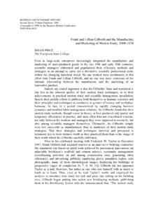
1 Spring 2007 Lecture 111 Lecture 11 Digital Circuits (I)THE INVERTERO utline Introduction to digital circuits The inverter NMOS inverter with resistor pull-upReading Assignment:Howe and Sodini; Chapter 5, Sections Spring 2007 Lecture 1121. Introduction to digital circuits: the inverter Logic 0:VMIN V VOL Logic 1:VOH V VMAX Undefined logic value:VOL V VOHIn digital circuits, digitally-encoded information is represented by means of two distinct voltage ranges:Logic operations are performed using logic logic operation of all: inversion inverterVlogic 1logic 0undefined regionVOLVMAXVMINVOHThe Static Spring 2007 Lecture 113 Ideal inverter VM input voltage for which VOUT= VIN For 0 VIN< VM VOUT= V+ For VM< VIN V+ VOUT= 0 Define switching pointor logic threshold:Circuit representation and ideal transfer function:Ideal inverter returns well defined logical outputs (0 or V+) even in the presence of considerable noise in VIN(from voltage spikes, crosstalk, etc.)
2 Signal is regenerated!v+++--VINVOUTVOUTVINV+V+V+2 VOUT=VINV+2VM=00 INOUT= Spring 2007 Lecture 114 Real inverter Logic 0: VMIN output voltage for which VIN= V+ VOL smallest output voltage where slope = -1 Logic 1: VOH largest output voltage where slope = -1 VMAX output voltage for which VIN= 0In a real inverter, valid logic levels defined as follows:VOUTVINV+00slope=-1 VOHVOLVMINVMAX logic 1logic 0transition Spring 2007 Lecture 115 Two other important voltages:Define:VIL smallest input voltage where slope = -1 VIH highest input voltage where slope = -1If range of output values VOLto VOHis widerthan the range of input values VILto VIH, then the inverter exhibits some noise immunity . (|Voltage gain| > 1)Quantify this through noise +00slope=-1 VOHVILVIHVOLVMINVMAX logic 1logic 0undefined regionrange of input valuesthat produce valid logic 0range of input valuesthat produce valid logic Spring 2007 Lecture 116 Chain of two inverters:Define noise margins:NMH VOH-VIHnoise margin highNML VIL-VOLnoise margin lownoiseMNinverter Moutputinverter Spring 2007 Lecture 117 Simplifications for hand calculations:Logic levels and noise margins Assume VOL VMINand VOH VMAX Trace tangent of transfer function at VM Slope = small signal voltage gain (Av) at VM VIL intersection of tangent with VOUT= VMAX VIH intersection of tangent with VOUT= VMINIt is hard to compute points in transfer function with slope = in the following way:VOUTVIHVILVMVMVINV+00 VOL=VMINVOH=VMAXVOUT=VINslope= Spring 2007 Lecture 118 Transient CharacteristicsInverter switching in the time domain.
3 TR rise timebetween 10% and 90% of total swingtF fall timebetween 90% and 10% of total swingtPHL propagation delay from high-to-lowbetween 50% pointstPLH propagation delay from low-to-highbetween 50% pointsPropagation delay :tP=12tPHL+tPLH()VOL90%50%10%tPHLtPLHVOH tRtCYCLE50%90%10% Spring 2007 Lecture 119 Simplifications for hand calculations:Propagation delay Consider input waveform is an ideal square wave Propagation delay times = delay times to 50% point SPICE essential for accurate delay analysisVOHVOHVOLVINVOUTtPHLtPLHVOHVOL50 % Spring 2007 Lecture 11102. NMOS inverter with pull-up resistor VBS= 0 (typically not shown) CLsummarizes capacitive loading of the following stages (other logic gates, interconnect lines, etc.) If VIN< VT, MOSFET is OFF VOUT= VDD If VIN> VT, MOSFET is ON VOUT small Value set by resistor / nMOS dividerBasic Operation:Essential features:VINVOUTV+=VDDIRIDCLR load capacitance(from followingstages) Spring 2007 Lecture 1111 Transfer function obtained by solving:IR= IDCan solve graphically: I V characteristics of load: VINVRVOUTVDDIRIDR+ Spring 2007 Lecture 1112 Overlap I V characteristics of resistor pull-up on I V characteristics of transistor:Transfer function:VDSVGS=VDDVGS=VINVGS=VT00IR=IDV DDVDDR load lineVOUT=VDSVIN=VGS00 VDDVTVDD= Spring 2007 Lecture 1113 For VMAX, transistor is cut-off, ID= 0:VMAX= VDDFor VMIN, transistor is in linear regime; solve: ID=WL nCoxVDD VMIN2 VT VMIN=IR=VDD VMINRID=W2L nCoxVM VT()2=IR=VDD VMRFor VM, transistor is in saturation.
4 Solve:Logic levels:VOUT=VDSVOUT=VINVIN=VGS00 VDDVTVMVMVMAX= Spring 2007 Lecture 1114 Small signal equivalent circuit model at VM(transistor in saturation): Av=voutvin= gmro//R() gmRNoise Margins:VOUT=VDSVOUT=VINVIN=VGS00 VDDVTVMAX=VDDVMINAvGSD+-vin+-vgs+-voutgm vgsroR+-vin+-voutgmvin(ro//R) Spring 2007 Lecture 1115 What did we learn today? Logic circuits must exhibit immunity to noise in the input signal noise margins Logic circuits must be regenerative Able to restore clean logic values even if input is noisy. Propagation delay: time for logic gate to perform its function. Concept of load line:graphical technique to visualize transfer characteristics of inverter. First-order solution (by hand) of inverter figures-of-merit easy if regions of operationof transistor are correctly identified. For more accurate solutions, use SPICE (or other CAD tool).Summary of Key Concepts