Transcription of Lecture 24 MOSFET Basics (Understanding with no math ...
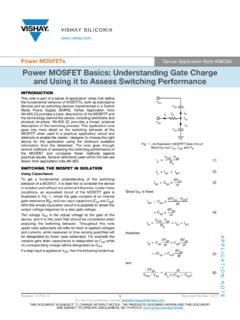
1 ECE 3040 - Dr. Alan DoolittleGeorgia TechLecture 24 MOSFET Basics (Understanding with no math) Reading: Pierret and Jaeger and NotesECE 3040 - Dr. Alan DoolittleGeorgia TechFlow of current from Source to Drain is controlled by the Gate by the Gate voltage is achieved by modulating the conductivity of the semiconductor region just below the gate. This region is known as the channelMOS TransistorQualitative DescriptionECE 3040 - Dr. Alan DoolittleGeorgia TechGSDBVGSVBSVDS+++-n-channel MOS TransistorG=Gate, D=Drain, S=Source, B=Body (substrate, but to avoid confusion with substrate, B is used)GSDBVSGVSBVSD---+p-channel MOS TransistorNote: All voltages are shown in their positive direction.
2 Obviously, VYX=-VXYfor any voltageMOS TransistorQualitative DescriptionECE 3040 - Dr. Alan DoolittleGeorgia TechP-typeMOS TransistorQualitative DescriptionAssume an n-channel (receives it s name from the type of channel present when current is flowing) device with its source and substrate grounded (i. e., VS=VB=0 V).For any value of VDS: when VGS<0 (accumulation), the source to drain path consists of two back to back diodes. One of these diodes is always reverse biased regardless of the drain voltage polarity. when VGS<VT(depletion), there is a deficit of electrons and holes making the channel very highly resistive. => No Drain current can due to DepletionECE 3040 - Dr.
3 Alan DoolittleGeorgia TechMOS TransistorQualitative DescriptionConsider now the Inversion case:First, VDS= 0: when VGS> VT, an induced n- type region, an inversion layer , forms in the channel and electrically connects the source and layer (n-type)ECE 3040 - Dr. Alan DoolittleGeorgia TechMOS TransistorQualitative DescriptionInversion case, VGS> VT(continued):When VDS>0 , the induced n- type region allows current to flow between the source and drain. The induced channel ast like a simple resistor. Thus, this current, ID, depends linearly on the Drain voltage VD. This mode of operation is called the linear or triode * layer (n-type)* Triode is a historical term from vacuum tube 3040 - Dr.
4 Alan DoolittleGeorgia TechInversion case, VGS> VT(continued):Drain current verses drain voltage when in the linear or triode * TransistorQualitative DescriptionECE 3040 - Dr. Alan DoolittleGeorgia TechMOS TransistorQualitative DescriptionInversion case, VGS> VT(continued):When VDSincreases a few tenths of a volt (>0): The depletion region near the drain widens (N+ drain is positively biased reverse biased with respect to the substrate). The electron concentration in the inversion layer near the drain decreases as they are sucked out by the Drain voltage. Channel conductance decreases resulting in a drop in the slope of the electron concentration in the Inversion layer near the drainECE 3040 - Dr.
5 Alan DoolittleGeorgia TechInversion case, VGS> VT(continued):Drain current verses drain voltage for increasing VDS(still in the linear or triode region).MOS TransistorQualitative DescriptionECE 3040 - Dr. Alan DoolittleGeorgia TechMOS TransistorQualitative DescriptionInversion case, VGS> VT(continued):The inversion layer eventually vanishes near the drain end of the is called Pinch-Off and results in a Flat ID-VDScurveECE 3040 - Dr. Alan DoolittleGeorgia TechInversion case, VGS> VT(continued):ID-VDScurve for the Saturation Region The drain-source voltage, VDS, at which this occurs is called the saturation voltage, Vsatwhile the current is called the saturation current, TransistorQualitative DescriptionIDsatECE 3040 - Dr.
6 Alan DoolittleGeorgia TechMOS TransistorQualitative DescriptionInversion case, VGS> VT(continued):For VDS>Vsatthe channel length, L, effectively changes by a value region of the channel, L is depleted and thus, is high resistivity. Accordingly, almost all voltage increases in VDS>Vsatare dropped across this portion of the electric fields in this region act similarly to the collector-base junction in a BJT in active mode, stripping or collecting carriers from the 3040 - Dr. Alan DoolittleGeorgia TechMOS TransistorQualitative DescriptionInversion case, VGS> VT(continued):If L<<L, the voltage at the end of the channel will be constant (Vsat) for all VDS>Vsat. IDwill be L~L, the voltage dropped across the the channel (VSAT) varies greatly with VDSdue to large modulations in the electric field across the pinched off region ( E=[VDS-VSAT]/[ L]).
7 In this case, IDincreases slightly with 3040 - Dr. Alan DoolittleGeorgia TechMOS TransistorQualitative DescriptionFinally, ID-VDScurves for various VGS:VDsatdepends on VGECE 3040 - Dr. Alan DoolittleGeorgia TechMOS Transistor vs MOS Capacitor Bias ModesMOS CapAccumulationDepletionInversionMOSFETC utoffLinear/TriodeSaturation0 VDSATVDSNMOSVTNVGSPMOSVTPVGS