Transcription of Lecture 4 - solidification
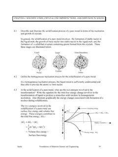
1 chapter 4 Solidificationand Crystalline Imperfectionsin Solids4-1 solidification of Metals Metals are melted to produce finished and semi-finished parts. Two steps of solidification Nucleation: Formation of stable nuclei. Growth of nuclei: Formation of grain structure. Thermal gradients define the shape of each grain. LiquidNucleiCrystals that willForm grainsGrain BoundariesGrains4-2 Figure of Stable Nuclei Two main mechanisms: Homogenousand heterogeneous. Homogenous Nucleation : First and simplest case. Metal itself will provide atoms to form nuclei. Metal, when significantly undercooled, has several slow moving atoms which bond each other to form nuclei. Cluster of atoms below critical sizeis called embryo. If the cluster of atoms reach critical size, they grow into crystals. Else get dissolved. Cluster of atoms that are grater than critical size are called nucleus. 4-3 Energies involved in homogenous free energy Gv Released by liquid to solid transformation.
2 Gvis change in free energy per unit volume between liquid and solid . free energy change for a spherical nucleus of radius r is given bySurface energy Gs Required to form new solid surface Gs is energy needed to create a surface. is specific surface free Gs is retarding energy. 2s4Gr= vGrr =334 4-4 Total Free Energy Total free energyis given by 23434rGrGvT+ = NucleusAbove criticalradius r*Below criticalradius r*Energy lowered bygrowing intocrystalsEnergyLowered byredissolvingVGr = 2*Since when r=r*, d( GT)/dr = 0r*r G+- Gv Gs GT4-4r*Figure Radius Versus Undercooling Greater the degree of undercooling, greater the change in volume free energy Gv Gs does not change significantly. As the amount of undercooling T increases, critical nucleus size decreases. Critical radius is related to undercooling by relation THTrfm = 2*r* = critical radius of nucleus = Surface free energy Hf= Latent heat of fusion T = Amount of Nucleation Nucleation occurs in a liquid on the surfaces of structural materials Eg:- Insoluble impurities.
3 These structures, called nucleating agents, lower the free energy required to form stable nucleus. Nucleating agents also lower the critical size. Smaller amount of undercooling is required to solidify. Used excessively in agent 4-7 Figure of Crystals and Formation of Grain Structure Nucleus grow into crystals in different orientations. Crystal boundariesare formed when crystals join together at complete solidification . Crystals in solidified metals are called grains. Grains are separated by grain boundaries. More the number of nucleation sites available, more the number of grains formed. Nuclei growing into grainsForming grain boundaries4-8 Types of Grains Equiaxed Grains: Crystals, smaller in size, grow equally in all directions. Formed at the sites of high concentration of the nuclie. Example:- Cold mold wall Columnar Grains: Long thin and coarse. Grow predominantly in one direction. Formed at the sites of slow coolingand steep temperature gradient.
4 Example:- Grains that are away fromthe mold GrainsEquiaxed GrainsMold4-9 Figure in Industries In industries, molten metal is cast into either semi finished or finished semicontinuousCasting unit for aluminumFigure castingOf steel ingotsGrain Structure in Industrial castings To produce cast ingots with fine grain size, grain refinersare added. Example:- For aluminum alloy, small amount of Titanium, Boron or Zirconium is added. 4-11 Figure (a)(b)Grain structure ofAluminum cast with (a) and without (b)grain Metals Handbook vol. 8, 8thed., American Society of Metals, 1973, ) solidification of Single Crystal For some applications (Eg: Gas turbine blades-high temperature environment), single crystalsare needed. Single crystals have high temperature creep resistance. Latent head of solidification is conducted through solidifying crystal to grow single crystal. Growth rate is kept slow so that temperature at solid -liquid interface is slightly below melting point.
5 4-12 Figure of singlecrystal for turbineairfoil.(After Pratt and Whitney Co.)Czochralski Process This method is used to produce single crystal of silicon for electronic wafers. A seed crystal is dipped in molten silicon and rotated. The seed crystal is withdrawn slowly while silicon adheres to seed crystal and grows as a single solid Solutions Alloys are used in most engineering applications. Alloyis an mixture of two or more metals and nonmetals. Example: Cartridge brassis binary alloy of 70% Cu and 30% Zinc. Iconelis a nickel based superalloy with about 10 elements. solid solution is a simple type of alloy in which elements are dispersed in a single phase. 4-14 Substitutional solid Solution Solute atoms substitutefor parent solvent atom in a crystal lattice. The structure remains unchanged. Lattice might get slightly distorteddue to change in diameter of the atoms. Solute percentage in solvent can vary from fraction of a percentage to 100%Solvent atomsSolute atoms4-15 Figure solid Solution ( ) The solubilityof solids is greater if The diameterof atoms not differ by more than 15% Crystal structures are similar.
6 No much difference in electronegativity(else compounds will be formed). Have some valence. Examples:-100% radiusDifferenceSystem4-16 Interstitial solid Solution Solute atoms fit in between the voids (interstices)of solvent atoms. Solvent atoms in this case should be much larger than solute atoms. Example:- between 912 and 13940C, interstitial solid solution of carbon in iron (FCC) is formed. A maximum of of carbon can dissolve interstitially in atoms r= atoms imperfections No crystal is perfect. imperfections affect mechanical properties, chemical properties and electrical properties. imperfections can be classified as Zero dimension point defects. One dimension / line defects (dislocations). Two dimension defects. Three dimension defects (cracks).4-18 Point Defects Vacancy Vacancy is formed due to a missing atom. Vacancy is formed (one in 10000 atoms) during crystallization or mobility of atoms. Energyof formation is 1 ev.
7 Mobility of vacancy results in cluster of vacancies. Also caused due to plastic defor--mation, rapid cooling or : Vacancies moving to form vacancy cluster4-19 Point Defects - Interstitially Atom in a crystal, sometimes, occupies interstitial site. This does not occur naturally. Can be induced by irradiation. This defects caused structural Defects in Ionic Crystals Complex as electric neutrality has to be maintained. If two appositely charged particles are missing, cation-anion divacancyis created. This is Schottky imperfection. Frenkelimperfection is created when cation moves to interstitial site. Impurity atoms are also considered as point Conduction Classical Model Metallic bondsmake free movement of valence electrons possible. Outer valence electrons are completely free to move between positive ion cores. Positive ion cores vibratewith greater amplitude with increasing temperature. The motion of electrons are random and restrictedin absence of electric field.
8 In presence of electric field, electrons attain directed drift Valence electrons are delocalized, interact and interpenetrateeach other. Their sharp energy levels are broadened into energy bands. Example:-Sodium has 1 valence electron (3S1). If there are N sodium atoms, there are N distinct3S1energy levels in 3S band. Sodium is a good conductor since it has half filled outer orbital In insulators, electrons are tightly energy gapEg Separates lower filled valence band and upper empty conduction be available for conduction, the electron should jump the energy s Law Ohm s lawstates that electric current flow I is directly proportional to the applied voltage V and inversely proportional to resistance of the wire:i = V/Rwhere i = electric current (A)V = potential difference (V)R = resistance of wire ( ) Electric resistivity = RA/ll= length of the conductorA = cross-sectional area of the conductor Electric Conductivity = 1/ SiliconGermaniumPolyethylenePolystyreneS ilverCopper GoldSemiconductorsInsulatorsConductors14 -3 Conduction in Intrinsic Semiconductors Semiconductors:Conductors between good conductors and insulators.
9 Intrinsic Semiconductors: Pure semiconductors and conductivity depends on inherent properties. Example:Silicon and Germanium each atom contributes 4 valence electrons for covalent bond. Valence electrons are excitedawayfrom their bondingposition when they are excited. Moved electron leaves Charge Transport in Pure Silicon Both electrons and holes are charge carriers. Hole is attractedto negative terminal, electron to the positive terminal Valence electron A is missing Hole Valence electron B movesto that spot due to the electric field leaving behind a hole. Movement of electrons is opposite to the electric Semiconductors Extrinsic semiconductors have impurity atoms(100-1000 ppm) that have different valance characteristics. n type extrinsic semiconductors: Impurities donate electrons for conduction. Example:-Group V A atoms ( P, As, Sb) added to silicon or SemiconductorsP-Type Extrinsic Semiconductors Group III A atoms when added to silicon, a hole is created since one of the bonding electrons is missing When electric field is applied, electrons from the neighboring bond moveto the hole Boron atom gets ionizedand hole moves towards negative terminal B, Al, provide acceptor levelenergy and are hence called acceptor atoms Doping:Impurity atoms (dopants) are deposited into silicon by diffusion at 11000C.
10 14-13 Line Defects (Dislocations) Lattice distortions are centeredaround a line. Formed during solidification Permanent Deformation Vacancy condensation Atomic mismatch Different types of line defects are Edge dislocation Screw dislocation Mixed dislocation 4-22 Edge Dislocation Created by insertion of extra half planesof atoms. Positive edge dislocation Negative edge dislocation Burgers vectorShows displa-cement of atoms (slip).4-23 Burgers vectorFigure Guy , Essentials of Materials Science, McGraw-Hill, 1976, M. Eisenstadt, Introduction to Mechanical Properties of Materials, Macmillan, 1971, Dislocation Created due to shear stressesapplied to regions of a perfect crystal separated by cutting plane. Distortion of lattice in form of a spiral ramp. Burgers vector is parallel to dislocation M. Eisenstadt, Introduction to Mechanical Properties of Materials, Macmillan, 1971, Dislocation Most crystal have componentsof bothedge and screw dislocation.