Transcription of LM118/LM218/LM318 Operational Amplifiers - …
1 LM118/LM218/LM318 Operational AmplifiersGeneral DescriptionThe LM118 series are precision high speed Operational am-plifiers designed for applications requiring wide bandwidthand high slew rate. They feature a factor of ten increase inspeed over general purpose devices without sacrificing LM118 series has internal unity gain frequency compen-sation. This considerably simplifies its application since noexternal components are necessary for operation. However,unlike most internally compensated Amplifiers , external fre-quency compensation may be added for optimum perfor-mance.
2 For inverting applications, feedforward compensa-tion will boost the slew rate to over 150V/ s and almostdouble the bandwidth. Overcompensation can be used withthe amplifier for greater stability when maximum bandwidthis not needed. Further, a single capacitor can be added to re-duce the settling time to under 1 high speed and fast settling time of these op amps makethem useful in A/D converters, oscillators, active filters,sample and hold circuits, or general purpose devices are easy to apply and offer an order of mag-nitude better AC performance than industry standards suchas the LM218 is identical to the LM118 except that the LM218has its performance specified over a 25 C to +85 C tem-perature range.
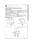
3 The LM318 is specified from 0 C to +70 MHz small signal bandwidthnGuaranteed 50V/ s slew ratenMaximum bias current of 250 nAnOperates from supplies of 5V to 20 VnInternal frequency compensationnInput and output overload protectednPin compatible with general purpose op ampsFast Voltage Follower(Note 1)DS007766-13 Note 1:Do not hard-wire as voltage follower (R1 5k )August 2000LM118/LM218/LM318 Operational Amplifiers 2000 National Semiconductor Maximum Ratings(Note 7)If Military/Aerospace specified devices are required,please contact the National Semiconductor Sales Office/Distributors for availability and Voltage 20 VPower Dissipation (Note 2)500 mWDifferential Input Current (Note 3) 10 mAInput Voltage (Note 4)
4 15 VOutput Short-Circuit DurationContinuousOperating Temperature RangeLM118 55 C to +125 CLM218 25 C to +85 CLM3180 C to +70 CStorage Temperature Range 65 C to +150 CLead Temperature (Soldering, 10 sec.)Hermetic Package300 CPlastic Package260 CSoldering InformationDual-In-Line PackageSoldering (10 sec.)260 CSmall Outline PackageVapor Phase (60 sec.)215 CInfrared (15 sec.)220 CSee AN-450 Surface Mounting Methods and Their Effecton Product Reliability for other methods of solderingsurface mount Tolerance (Note 8)2000 VElectrical Characteristics(Note 5)ParameterConditionsLM118/LM218LM318 UnitsMinTypMaxMinTypMaxInput Offset VoltageTA= 25 C24410mVInput Offset CurrentTA= 25 C65030200nAInput Bias CurrentTA= 25 C120250150500nAInput ResistanceTA= 25 Supply CurrentTA= 25 C58510mALarge Signal Voltage GainTA= 25 C, VS= 15V5020025200V/mVVOUT= 10V, RL 2k Slew RateTA= 25 C, VS= 15V, AV= 150705070V/ s(Note 6)
5 Small Signal BandwidthTA= 25 C, VS= 15V1515 MHzInput Offset Voltage615mVInput Offset Current100300nAInput Bias Current500750nASupply CurrentTA= 125 Signal Voltage GainVS= 15V, VOUT= 10V2520V/mVRL 2k Output Voltage SwingVS= 15V, RL=2k 12 13 12 13 VInput Voltage RangeVS= 15V Rejection Ratio8010070100dBSupply Voltage Rejection Ratio70806580dBNote 2:The maximum junction temperature of the LM118 is 150 C, the LM218 is 110 C, and the LM318 is 110 C. For operating at elevated temperatures, devicesin the H08 package must be derated based on a thermal resistance of 160 C/W, junction to ambient, or 20 C/W, junction to case.
6 The thermal resistance ofthedual-in-line package is 100 C/W, junction to 3:The inputs are shunted with back-to-back diodes for overvoltage protection. Therefore, excessive current will flow if a differential input voltagein excess of1V is applied between the inputs unless some limiting resistance is 4:For supply voltages less than 15V, the absolute maximum input voltage is equal to the supply 5:These specifications apply for 5V VS 20V and 55 C TA +125 C (LM118), 25 C TA +85 C (LM218), and 0 C TA +70 C (LM318). Also,power supplies must be bypassed with F disc 6:Slew rate is tested with VS= 15V.
7 The LM118 is in a unity-gain non-inverting configuration. VINis stepped from to + and vice versa. The slewrates between and + and vice versa are tested and guaranteed to exceed 50V/ 7:Refer to RETS118X for LM118H and LM118J military 8:Human body model, k in series with 100 Performance CharacteristicsLM118, LM218 Input CurrentDS007766-25 Voltage GainDS007766-26 Power Supply RejectionDS007766-27 Input Noise VoltageDS007766-28 Common Mode RejectionDS007766-29 Supply CurrentDS007766-30 Closed Loop OutputImpedanceDS007766-31 Current LimitingDS007766-32 Input CurrentDS007766-33 Unity Gain BandwidthDS007766-34 Voltage Follower Slew RateDS007766-35 Inverter Settling TimeDS007766-36LM118/LM218 Performance CharacteristicsLM118, LM218 (Continued)
8 Typical Performance CharacteristicsLM318 Large Signal FrequencyResponseDS007766-37 Open Loop FrequencyResponseDS007766-38 Voltage Follower PulseResponseDS007766-39 Large Signal FrequencyResponseDS007766-40 Open Loop FrequencyResponseDS007766-41 Inverter Pulse ResponseDS007766-42 Input CurrentDS007766-43 Voltage GainDS007766-44 Power Supply RejectionDS007766-45LM118/LM218 Performance CharacteristicsLM318 (Continued)Input Noise VoltageDS007766-46 Common Mode RejectionDS007766-47 Supply CurrentDS007766-48 Closed Loop Output ImpedanceDS007766-49 Current LimitingDS007766-50 Input CurrentDS007766-51 Unity Gain BandwidthDS007766-52 Voltage Follower Slew RateDS007766-53 Inverter Settling TimeDS007766-54LM118/LM218 Performance CharacteristicsLM318 (Continued)Auxiliary CircuitsNote 10.
9 Slew and settling time to for a 10V step change is 800 Signal FrequencyResponseDS007766-55 Open Loop FrequencyResponseDS007766-56 Voltage Follower PulseResponseDS007766-57 Large Signal FrequencyResponseDS007766-58 Open Loop FrequencyResponseDS007766-59 Inverter Pulse ResponseDS007766-60 Feedforward Compensationfor Greater Inverting Slew Rate(Note 9)DS007766-8*Balance circuit necessary for increased 9:Slew rate typically 150V/ for Minimum Settling Time(Note 10)DS007766-9LM118/LM218 Circuits(Continued)Typical ApplicationsOffset BalancingDS007766-10 Isolating Large Capacitive LoadsDS007766-11 OvercompensationDS007766-12 Fast Voltage Follower(Note 11)DS007766-13 Integrator or Slow InverterDS007766-14CF= Large(CF 50 pF)*Do not hard-wire as integrator or slow inverter.
10 Insert a 10k-5 pF networkin series with the input, to prevent 11:Do not hard-wire as voltage follower (R1 5k )Fast Summing AmplifierDS007766-15 Differential AmplifierDS007766-16LM118/LM218 Applications(Continued)Fast Sample and HoldDS007766-18D/A Converter Using Ladder NetworkDS007766-19*Optional Reduces settling Applications(Continued)Four Quadrant MultiplierDS007766-17 Output zero.* Y zero+ X zero Full scale Applications(Continued)D/A Converter Using Binary Weighted NetworkDS007766-20*Optional Reduces settling Summing Amplifier with Low Input CurrentDS007766-21 Wein Bridge Sine Wave OscillatorDS007766-22 Instrumentation AmplifierDS007766-23LM118/LM218 DiagramDS007766-1LM118/LM218 DiagramNote 12:Pin connections shown on schematic diagram and typical applications are for TO-5 13.