Transcription of LM258, LM358, LM358A, LM358E, LM2904, …
1 Semiconductor Components Industries, LLC, 2016 October, 2016 Rev. 321 Publication Order Number: lm358 /DLM258, lm358 , LM358A, lm358e , lm2904 , lm2904a , lm2904e , LM2904V,NCV2904 single supply DualOperational AmplifiersUtilizing the circuit designs perfected for Quad OperationalAmplifiers, these dual operational amplifiers feature low power drain,a common mode input voltage range extending to ground/VEE, andsingle supply or split supply operation. The lm358 series isequivalent to one half of an amplifiers have several distinct advantages over standardoperational amplifier types in single supply applications.
2 They canoperate at supply voltages as low as V or as high as 32 V, withquiescent currents about one fifth of those associated with theMC1741 (on a per amplifier basis). The common mode input rangeincludes the negative supply , thereby eliminating the necessity forexternal biasing components in many applications. The output voltagerange also includes the negative power supply Short Circuit Protected Outputs True Differential Input Stage single supply Operation: V to 32 V Low Input Bias Currents Internally Compensated Common Mode Range Extends to Negative supply single and Split supply Operation ESD Clamps on the Inputs Increase Ruggedness of the Devicewithout Affecting Operation NCV Prefix for Automotive and Other Applications RequiringUnique Site and Control Change Requirements.
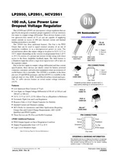
3 AEC Q100 Qualified and PPAP Capable These Devices are Pb Free, Halogen Free/BFR Free and are RoHSCompliantPDIP 8N, AN, VN SUFFIXCASE 62618 SOIC 8D, VD SUFFIXCASE 75118 PIN CONNECTIONS VEE/GndInputs AInputs BOutput BOutput A VCC ++12348765(Top View)See general marking information in the device markingsection on page 11 of this data MARKING INFORMATIONSee detailed ordering and shipping information in the packagedimensions section on page 10 of this data INFORMATIONM icro8]DMR2 SUFFIXCASE , lm358 , lm358a , lm358e , lm2904 , lm2904a , lm2904e , LM2904V, SupplySplit V to VCC(max) V to VCC(max) V to VEE(max)OutputBias CircuitryCommon to kQ25Q2240 kQ24Q23Q1225 Figure 1.
4 Figure 2. Representative Schematic Diagram(One Half of Circuit Shown) lm258 , lm358 , lm358a , lm358e , lm2904 , lm2904a , lm2904e , LM2904V, RATINGS (TA = +25 C, unless otherwise noted.)RatingSymbolValueUnitPower supply VoltagesSingle SupplySplit SuppliesVCCVCC, VEE32 16 VdcInput Differential Voltage Range (Note 1)VIDR 32 VdcInput Common Mode Voltage RangeVICR to 32 VdcOutput Short Circuit DurationtSCContinuousJunction TemperatureTJ150 CThermal Resistance, Junction to Air (Note 2)Case 846 ACase 751 Case 626R JA238212161 C/WStorage Temperature RangeTstg 65 to +150 COperating Ambient Temperature RangeLM258LM358, lm358a , lm358 ELM2904, lm2904a , lm2904 ELM2904V, NCV2904 (Note 3)TA 25 to +850 to +70 40 to +105 40 to +125 CStresses exceeding those listed in the Maximum Ratings table may damage the device.
5 If any of these limits are exceeded, device functionalityshould not be assumed, damage may occur and reliability may be Split Power All R JA measurements made on evaluation board with 1 oz. copper traces of minimum pad size. All device outputs were is qualified for automotive RATINGSR atingHBMMMUnitESD Protection at any Pin (Human Body Model HBM, Machine Model MM)NCV2904 (Note 3) lm358e , lm2904 ELM358DG/DR2G, LM2904DG/DR2 GAll Other Devices200020002502000200200100200 VVVVLM258, lm358 , lm358a , lm358e , lm2904 , lm2904a , lm2904e , LM2904V, CHARACTERISTICS (VCC = V, VEE = GND, TA = 25 C, unless otherwise noted.)CharacteristicSymbolLM258LM358, lm358 ELM358 AUnitMinTypMaxMinTypMaxMinTypMaxInput Offset VoltageVCC = V to 30 V, VIC = 0 V to VCC V,VO ] V, RS = 0 VIOmVTA = 25 C = Thigh (Note 4) = Tlow (Note 4) Temperature Coefficient of Input OffsetVoltage VIO/ T V/ CTA = Thigh to Tlow (Note 4)Input Offset CurrentIIO = Thigh to Tlow (Note 4) 100 150 75 Input Bias CurrentIIB 45 150 45 250 45 100TA = Thigh to Tlow (Note 4) 50 300 50 500 50 200 Average Temperature Coefficient of Input OffsetCurrent IIO/ T 10 10 10 pA/ CTA = Thigh to Tlow (Note 4)Input Common Mode Voltage Range (Note 5)
6 ,VCC = 30 VVICR0 = 30 V, TA = Thigh to Tlow0 280 280 28 Differential Input Voltage RangeVIDR VCC VCC VCCVL arge Signal Open Loop Voltage GainAVOLV/mVRL = k , VCC = 15 V, For Large VO Swing,50100 25100 25100 TA = Thigh to Tlow (Note 4)25 15 15 Channel SeparationCS 120 120 120 kHz f 20 kHz, Input ReferencedCommon Mode RejectionCMR7085 6570 6570 dBRS 10 k Power supply RejectionPSR65100 65100 65100 dBOutput Voltage High Limit TA = Thigh to Tlow (Note 4)VOHVVCC = V, RL = k , TA = 25 VCC = 30 V, RL = k 26 26 26 VCC = 30 V, RL = 10 k 2728 2728 2728 Output Voltage Low LimitVOL = V, RL = 10 k , TA = Thigh to Tlow (Note 4)Output Source CurrentIO +mAVID = + V, VCC = 15 V2040 2040 2040 TA = Thigh to Tlow ( lm358a Only)10 Output Sink CurrentIO VID = V, VCC = 15 V1020 1020 1020 mATA = Thigh to Tlow ( lm358a Only) mAVID = V, VO = 200 mV1250 1250 1250 AOutput Short Circuit to Ground (Note 6)ISC 4060 4060 4060mAPower supply Current (Total Device)TA = Thigh to Tlow (Note 4)ICCmAVCC = 30 V, VO = 0 V, RL = = 5 V, VO = 0 V, RL = lm258 .
7 Tlow = 25 C, Thigh = +85 CLM358, lm358a , lm358e : Tlow = 0 C, Thigh = +70 CLM2904/A/E: Tlow = 40 C, Thigh = +105 CLM2904V & NCV2904: Tlow = 40 C, Thigh = +125 CNCV2904 is qualified for automotive The input common mode voltage or either input signal voltage should not be allowed to go negative by more than V. The upper end ofthe common mode voltage range is VCC Short circuits from the output to VCC can cause excessive heating and eventual destruction. Destructive dissipation can result fromsimultaneous shorts on all , lm358 , lm358a , lm358e , lm2904 , lm2904a , lm2904e , LM2904V, CHARACTERISTICS (VCC = V, VEE = Gnd, TA = 25 C, unless otherwise noted.)
8 CharacteristicSymbolLM2904/ lm2904 ELM2904 ALM2904V, NCV2904 UnitMinTypMaxMinTypMaxMinTypMaxInput Offset VoltageVCC = V to 30 V, VIC = 0 V to VCC V,VO ] V, RS = 0 VIOmVTA = 25 C = Thigh (Note 7) 10 10 13TA = Tlow (Note 7) 10 10 10 Average Temperature Coefficient of Input OffsetVoltage VIO/ T V/ CTA = Thigh to Tlow (Note 7)Input Offset CurrentIIO = Thigh to Tlow (Note 7) 45200 45200 45200 Input Bias CurrentIIB 45 250 45 100 45 250TA = Thigh to Tlow (Note 7) 50 500 50 250 50 500 Average Temperature Coefficient of Input OffsetCurrent IIO/ T 10 10 10 pA/ CTA = Thigh to Tlow (Note 7)Input Common Mode Voltage Range (Note 8),VCC = 30 VVICR0 = 30 V, TA = Thigh to Tlow0 280 280 28 Differential Input Voltage RangeVIDR VCC VCC VCCVL arge Signal Open Loop Voltage GainAVOLV/mVRL = k , VCC = 15 V, For Large VO Swing,25100 25100 25100 TA = Thigh to Tlow (Note 7)15 15 15 Channel SeparationCS 120 120 120 kHz f 20 kHz, Input ReferencedCommon Mode RejectionCMR5070 5070 5070 dBRS 10 k Power supply RejectionPSR50100 50100 50100 dBOutput Voltage High Limit TA = Thigh to Tlow (Note 7)
9 VOHVVCC = V, RL = k , TA = 25 VCC = 30 V, RL = k 26 26 26 VCC = 30 V, RL = 10 k 2728 2728 2728 Output Voltage Low LimitVOL = V, RL = 10 k , TA = Thigh to Tlow (Note 7)Output Source CurrentIO +2040 2040 2040 mAVID = + V, VCC = 15 VOutput Sink CurrentIO VID = V, VCC = 15 V1020 1020 1020 mAVID = V, VO = 200 mV AOutput Short Circuit to Ground (Note 9)ISC 4060 4060 4060mAPower supply Current (Total Device)TA = Thigh to Tlow (Note 7)ICCmAVCC = 30 V, VO = 0 V, RL = = 5 V, VO = 0 V, RL = lm258 : Tlow = 25 C, Thigh = +85 CLM358, lm358a , lm358e : Tlow = 0 C, Thigh = +70 CLM2904/A/E: Tlow = 40 C, Thigh = +105 CLM2904V & NCV2904: Tlow = 40 C, Thigh = +125 CNCV2904 is qualified for automotive The input common mode voltage or either input signal voltage should not be allowed to go negative by more than V.
10 The upper end ofthe common mode voltage range is VCC Short circuits from the output to VCC can cause excessive heating and eventual destruction. Destructive dissipation can result fromsimultaneous shorts on all parametric performance is indicated in the Electrical Characteristics for the listed test conditions, unless otherwise noted. Productperformance may not be indicated by the Electrical Characteristics if operated under different , lm358 , lm358a , lm358e , lm2904 , lm2904a , lm2904e , LM2904V, DESCRIPTIONThe lm358 series is made using two internallycompensated, two stage operational amplifiers.
