Transcription of LM339 - Single Supply Quad Comparators
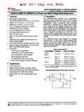
1 LM339 , LM339E, LM239, LM2901, LM2901E, LM2901V, NCV2901, MC3302. Single Supply quad Comparators These Comparators are designed for use in level detection, low level sensing and memory applications in consumer, automotive, and industrial electronic applications. SOIC 14. 14 D SUFFIX. Features CASE 751A. 1. Single Supply Operation: V to 36 V. Split Supply Operation: V to 18 V. Low Input Bias Current: 25 nA (Typ) PDIP 14. Low Input Offset Current: nA (Typ) N, P SUFFIX. CASE 646. Low Input Offset Voltage 14. Input Common Mode Voltage Range to GND 1. Low Output Saturation Voltage: 130 mV (Typ) @ mA. TTL and CMOS Compatible ESD Clamps on the Inputs Increase Reliability without Affecting TSSOP 14. Device Operation 14 DTB SUFFIX. NCV Prefix for Automotive and Other Applications Requiring CASE 948G. 1. Unique Site and Control Change Requirements; AEC Q100. Qualified and PPAP Capable These Devices are Pb Free, Halogen Free/BFR Free and are RoHS PIN CONNECTIONS. Compliant Output 2 1 14 Output 3.
2 Output 1 2 13 Output 4. VCC 3 12 GND. - Input 1 4 11 + Input 4. * ). 1 4. + Input 1 5. ) * 10 - Input 4. - Input 2 6 9 + Input 3. *2 ). 3. ) *. + Input 2 7 8 - Input 3. (Top View). ORDERING INFORMATION. See detailed ordering and shipping information in the package dimensions section on page 7 of this data sheet. DEVICE MARKING INFORMATION. See general marking information in the device marking section on page 8 of this data sheet. Semiconductor Components Industries, LLC, 2016 1 Publication Order Number: July, 2018 Rev. 25 LM339 /D. LM339 , LM339E, LM239, LM2901, LM2901E, LM2901V, NCV2901, MC3302. MAXIMUM RATINGS. Rating Symbol Value Unit Power Supply Voltage VCC Vdc LM239/ LM339 , E/LM2901, E, V +36 or 18. MC3302 +30 or 15. Input Differential Voltage Range VIDR Vdc LM239/ LM339 , E/LM2901, E, V 36. MC3302 30. Input Common Mode Voltage Range VICMR to 36 Vdc Output Short Circuit to Ground (Note 1) ISC Continuous Power Dissipation @ TA = 25 C PD. Plastic Package W. Derate above 25 C 1/RqJA mW/ C.
3 Junction Temperature TJ 150 C. Operating Ambient Temperature Range TA C. LM239 25 to +85. MC3302 40 to +85. LM2901, LM2901E 40 to +105. 40 to +125. LM2901V, NCV2901. 0 to +70. LM339 , LM339E. Storage Temperature Range Tstg 65 to +150 C. Stresses exceeding those listed in the Maximum Ratings table may damage the device. If any of these limits are exceeded, device functionality should not be assumed, damage may occur and reliability may be affected. 1. The maximum output current may be as high as 20 mA, independent of the magnitude of VCC. Output short circuits to VCC can cause excessive heating and eventual destruction. ESD RATINGS. Rating HBM MM Unit ESD Protection at any Pin (Human Body Model HBM, Machine Model MM). NCV2901 2000 200 V. LM339E, LM2901E 1500 200 V. LM339DG/DR2G, LM2901DG/DR2G 250 100 V. All Other Devices 1500 200 V. VCC + Input - Input Output GND. NOTE: Diagram shown is for 1 comparator. Figure 1. Circuit Schematic 2. LM339 , LM339E, LM239, LM2901, LM2901E, LM2901V, NCV2901, MC3302.
4 ELECTRICAL CHARACTERISTICS (VCC = + Vdc, TA = +25 C, unless otherwise noted). LM2901/2901E/2901V. LM239/339/339E /NCV2901 MC3302. Characteristic Symbol Min Typ Max Min Typ Max Min Typ Max Unit Input Offset Voltage (Note 3) VIO 20 mVdc Input Bias Current (Notes 3, 4) IIB 25 250 25 250 25 500 nA. (Output in Analog Range). Input Offset Current (Note 3) IIO 50 50 100 nA. Input Common Mode Voltage Range VICMR 0 VCC 0 VCC 0 VCC V. (Note 5) Supply Current ICC mA. RL = (For All Comparators ) RL = , VCC = 30 Vdc Voltage Gain AVOL 50 200 25 100 25 100 V/mV. RL 15 kW, VCC = 15 Vdc Large Signal Response Time 300 300 300 ns VI = TTL Logic Swing, Vref = Vdc, VRL = Vdc, RL = kW. Response Time (Note 6) ms VRL = Vdc, RL = kW. Output Sink Current ISink 16 16 16 mA. VI ( ) + Vdc, VI(+) = 0, VO Vdc Saturation Voltage Vsat 130 400 130 400 130 500 mV. VI( ) + Vdc, VI(+) = 0, Isink mA. Output Leakage Current IOL nA. VI(+) + Vdc, VI( ) = 0, VO = + Vdc Product parametric performance is indicated in the Electrical Characteristics for the listed test conditions, unless otherwise noted.
5 Product performance may not be indicated by the Electrical Characteristics if operated under different conditions. 2. (LM239) Tlow = 25 C, Thigh = +85 . ( LM339 , LM339E) Tlow = 0 C, Thigh = +70 C. (MC3302) Tlow = 40 C, Thigh = +85 C. (LM2901), LM2901E Tlow = 40 C, Thigh = +105 . (LM2901V & NCV2901) Tlow = 40 C, Thigh = +125 C. NCV2901 is qualified for automotive use. 3. At the output switch point, VO ] Vdc, RS 100 W Vdc VCC 30 Vdc, with the inputs over the full common mode range (0 Vdc to VCC Vdc). 4. The bias current flows out of the inputs due to the PNP input stage. This current is virtually constant, independent of the output state. 5. Positive excursions of input voltage may exceed the power Supply level. As long as one input voltage remains within the common mode range, the comparator will provide a proper output state. Refer to the Maximum Ratings table for safe operating area. 6. The response time specified is for a 100 mV input step with mV overdrive. For larger signals, 300 ns is typical.
6 3. LM339 , LM339E, LM239, LM2901, LM2901E, LM2901V, NCV2901, MC3302. PERFORMANCE CHARACTERISTICS (VCC = + Vdc, TA = Tlow to Thigh [Note 7]). LM2901/2901E/2901V. LM239/339/339E /NCV2901 MC3302. Characteristic Symbol Min Typ Max Min Typ Max Min Typ Max Unit Input Offset Voltage (Note 8) VIO 15 40 mVdc Input Bias Current (Notes 8, 9) IIB 400 500 1000 nA. (Output in Analog Range). Input Offset Current (Note 8) IIO 150 200 300 nA. Input Common Mode Voltage Range VICMR 0 VCC 0 VCC 0 VCC V. Saturation Voltage Vsat 700 700 700 mV. VI( ) + Vdc, VI(+) = 0, Isink mA. Output Leakage Current IOL mA. VI(+) + Vdc, VI( ) = 0, VO = 30 Vdc Differential Input Voltage VID VCC VCC VCC Vdc All VI 0 Vdc 7. (LM239) Tlow = 25 C, Thigh = +85 . ( LM339 , LM339E) Tlow = 0 C, Thigh = +70 C. (MC3302) Tlow = 40 C, Thigh = +85 C. (LM2901, LM2901E) Tlow = 40 C, Thigh = +105 . (LM2901V & NCV2901) Tlow = 40 C, Thigh = +125 C. NCV2901 is qualified for automotive use. 8. At the output switch point, VO ] Vdc, RS 100 W Vdc VCC 30 Vdc, with the inputs over the full common mode range (0 Vdc to VCC Vdc).
7 9. The bias current flows out of the inputs due to the PNP input stage. This current is virtually constant, independent of the output state. + VCC + VCC. R3. 10 k Rref 10 k Vin - Vref Rref VO 10 k + VCC +. R1 - R2 R2 VO. Vref Vin +. M 10 k 10k R1 VCC R1. Vref [ R3 VCC R1. Rref + R1 Vref =. M Rref + R1. R3 ] R1 / / Rref / / R2. R2 [ R1 / / Rref R1 / / Rref VH = [VO(max) - VO(min)] Amount of Hysteresis VH. R1/ / Rref + R2. R2. VH = [(V -V ]. R2 Rref / / R1 R2 + R3 O(max) O(min). Figure 2. Inverting Comparator Figure 3. Noninverting Comparator with Hysteresis with Hysteresis 4. LM339 , LM339E, LM239, LM2901, LM2901E, LM2901V, NCV2901, MC3302. Typical Characteristics (VCC = 15 Vdc, TA = +25 C (each comparator) unless otherwise noted.). 48. NORMALIZED OFFSET VOLTAGE. 42. I IB, INPUT BIAS CURRENT (nA). 36 TA = -55 C. TA = +25 C. 30. 24 TA = +125 C. 18. 12. 0. -50 -25 0 25 50 75 100 125 0 12 16 20 24 28 32. TA, AMBIENT TEMPERATURE ( C) VCC, POWER Supply VOLTAGE (Vdc). Figure 4.)]
8 Normalized Input Offset Voltage Figure 5. Input Bias Current IO, OUTPUT CURRENT (mA). TA = +25 C. TA = -55 C. TA = +125 C. 0. 0 100 200 300 400 500. Vsat, OUTPUT SATURATION VOLTAGE (mV). Figure 6. Output Sink Current versus Output Saturation Voltage VCC VCC V. 10 k 100 k RS RL. Vin + R1. - Vref - +. C VO. R1 +. VCC. R2 R3. VCC. RS = Source Resistance 330 k 330 k R4 330 k T1. R1 ] RS T2. T1 = T2 = RC. VCC RL. Logic Device (V) kW f[. C(mF). CMOS 1/4 MC14001 +15 100. R2 = R3 = R4. TTL 1/4 MC7400 + 10. R1 [ R2 // R3 // R4. Figure 7. Driving Logic Figure 8. Squarewave Oscillator 5. LM339 , LM339E, LM239, LM2901, LM2901E, LM2901V, NCV2901, MC3302. APPLICATIONS INFORMATION. These quad Comparators feature high gain, wide addition of positive feedback (< 10 mV) is also bandwidth characteristics. This gives the device oscillation recommended. It is good design practice to ground all tendencies if the outputs are capacitively coupled to the unused input pins. inputs via stray capacitance.]
9 This oscillation manifests itself Differential input voltages may be larger than Supply during output transitions (VOL to VOH). To alleviate this voltages without damaging the comparator's inputs. situation input resistors < 10 kW should be used. The Voltages more negative than 300 mV should not be used. +15 V. R1 R4 R5. 220 k 220 k 10 k Vin(min) V peak for 1% phase distortion (Dq). k Vin *. k VO Vin(min). ) Vin D1 R2. VCC q 15 k 10 M. R3. * 10 k VO. Vin + VCC. D1 prevents input from going negative by more than V. R1 + R2 = R3 VO q R5 VEE. R3 for small error in zero crossing Dq 10 VEE. Figure 9. Zero Crossing Detector Figure 10. Zero Crossing Detector ( Single Supply ) (Split Supplies). 6. LM339 , LM339E, LM239, LM2901, LM2901E, LM2901V, NCV2901, MC3302. ORDERING INFORMATION. Device Package Shipping . LM239DG SOIC 14 (Pb Free) 55 Units/Tube LM239DR2G SOIC 14 (Pb Free) 2500 / Tape & Reel LM239 DTBR2G TSSOP 14 (Pb Free) 2500 / Tape & Reel LM239NG PDIP 14 (Pb Free) 25 Units/Rail LM339DG SOIC 14 (Pb Free) 55 Units/Tube LM339DR2G SOIC 14 (Pb Free) 2500 / Tape & Reel LM339 EDR2G SOIC 14 (Pb Free) 2500 / Tape & Reel LM339 DTBR2G TSSOP 14 (Pb Free) 2500 / Tape & Reel LM339NG PDIP 14 (Pb Free) 25 Units/Rail LM2901DG SOIC 14 (Pb Free) 55 Units/Rail LM2901DR2G SOIC 14 (Pb Free) 2500 / Tape & Reel LM2901 EDR2G SOIC 14 (Pb Free) 2500 / Tape & Reel LM2901 DTBR2G TSSOP 14 (Pb Free) 2500 / Tape & Reel LM2901NG PDIP 14 (Pb Free) 25 Units/Rail LM2901 VDG SOIC 14 (Pb Free) 55 Units/Tube LM2901 VDR2G SOIC 14 (Pb Free) 2500 / Tape & Reel LM2901 VDTBR2G TSSOP 14 (Pb Free) 2500 / Tape & Reel LM2901 VNG PDIP 14 (Pb Free) 25 Units/Rail NCV2901DR2G* SOIC 14 (Pb Free) 2500 / Tape & Reel NCV2901 DTBR2G* TSSOP 14 (Pb Free)
10 2500 / Tape & Reel NCV2901 CTR* Bare Die 6000 / Tape & Reel MC3302DG SOIC 14 (Pb Free) 55 Units/Tube MC3302DR2G SOIC 14 (Pb Free) 2500 / Tape & Reel MC3302 DTBR2G TSSOP 14 (Pb Free) 2500 / Tape & Reel MC3302PG PDIP 14 (Pb Free) 25 Units/Rail For information on tape and reel specifications, including part orientation and tape sizes, please refer to our Tape and Reel Packaging Specifications Brochure, BRD8011/D. *NCV Prefix for Automotive and Other Applications Requiring Unique Site and Control Change Requirements; AEC Q100 Qualified and PPAP. Capable. 7. LM339 , LM339E, LM239, LM2901, LM2901E, LM2901V, NCV2901, MC3302. MARKING DIAGRAMS. PDIP 14. N, P SUFFIX. CASE 646. 14 14 14 14 14. LM339N LM239N LM2901N LM2901VN MC3302P. AWLYYWWG AWLYYWWG AWLYYWWG AWLYYWWG AWLYYWWG. 1 1 1 1 1. SOIC 14. D SUFFIX. CASE 751A. 14 14 14 14 14. LM339DG LM239DG LM2901DG LM2901 VDG * MC3302DG. AWLYWW AWLYWW AWLYWW AWLYWW AWLYWW. 1 1 1 1 1. 14 14. LM339EG LM2901EG. AWLYWW AWLYWW. 1 1. TSSOP 14. DTB SUFFIX.