Transcription of Low Cost, DC to 500 MHz, 92 dB Logarithmic Amplifier Data ...
1 Low Cost, DC to 500 MHz, 92 dBLogarithmic AmplifierData Sheet AD8307 Rev. E Document Feedback Information furnished by Analog Devices is believed to be accurate and reliable. However, no responsibility is assumed by Analog Devices for its use, nor for any infringements of patents or other rights of third parties that may result from its use. Specifications subject to change without notice. No license is granted by implication or otherwise under any patent or patent rights of Analog Devices. Trademarks and registered trademarks are the property of their respective owners. One Technology Way, Box 9106, Norwood, MA 02062-9106, : 1997 2015 Analog Devices, Inc. All rights reserved.
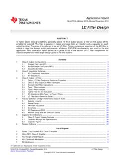
2 Technical Support FEATURES Complete multistage Logarithmic Amplifier 92 dB dynamic range: 75 dBm to +17 dBm to 90 dBm using matching network Single supply of V minimum at mA typical DC to 500 MHz operation, 1 dB linearity Slope of 25 mV/dB, intercept of 84 dBm Highly stable scaling over temperature Fully differential dc-coupled signal path 100 ns power-up time, 150 A sleep current APPLICATIONS Conversion of signal level to decibel form Transmitter antenna power measurement Receiver signal strength indication (RSSI) Low cost radar and sonar signal processing Network and spectrum analyzers (to 120 dB) Signal level determination down to 20 Hz True decibel ac mode for multimeters FUNCTIONAL BLOCK DIAGRAM BAND GAP REFERENCEAND BIASINGSIX 900 MHzAMPLIFIER STAGESMIRRORINPUT-OFFSETCOMPENSATION 322 COMNINE DETECTOR CELLSSPACED INP+INP8127564301082-001 Figure 1.
3 GENERAL DESCRIPTION The AD8307 is the first Logarithmic Amplifier made available in an 8-lead SOIC_N package. It is a complete 500 MHz monolithic demodulating Logarithmic Amplifier based on the progressive compression (successive detection) technique, providing a dynamic range of 92 dB to 3 dB law conformance and 88 dB to a tight 1 dB error bound at all frequencies up to 100 MHz. The AD8307 is extremely stable and easy to use, requiring no significant external components. A single-supply voltage of V to V at mA is needed. A fast acting CMOS-compatible control pin can disable the AD8307 to a standby current of 150 A. The AD8307 operates over the industrial temperature range of 40 C to +85 C and is available in an 8-lead SOIC package and an 8-lead PDIP.
4 Table 1. Next Generation Upgrades for the AD8307 Device No. Product Description AD8310 15 ns Response Time, Buffered Output ADL5513 Lower Input Range (80 dB), Operation to 4 GHz, Higher Power Consumption AD8309 Higher Input Range (100 dB), Limiter Output AD8307 Data Sheet Rev. E | Page 2 of 24 TABLE OF CONTENTS Features .. 1 Applications .. 1 Functional Block Diagram .. 1 General Description .. 1 Revision History .. 2 Specifications .. 3 Absolute Maximum Ratings .. 4 ESD Caution .. 4 Pin Configuration and Function Descriptions .. 5 Typical Performance Characteristics .. 6 Log Amp Theory .. 9 Progressive Compression .. 10 Demodulating Log Amps .. 11 Intercept Calibration .. 12 Offset Control .. 12 Extension of Range.
5 13 Interfaces .. 14 Enable Interface .. 14 Input Interface .. 14 Offset Interface .. 15 Output Interface .. 15 Theory of Operation .. 17 Basic Connections .. 17 Input Matching .. 18 Narrow-Band Matching .. 18 Slope and Intercept Adjustments .. 19 Applications Information .. 20 Buffered Output .. 20 Four-Pole Filter .. 20 1 W to 1 kW 50 Power Meter .. 21 Measurement System with 120 dB Dynamic Range .. 21 Operation at Low Frequencies .. 22 Outline Dimensions .. 23 Ordering Guide .. 24 REVISION HISTORY 9/15 Rev. D to Rev. E Changes to General Description Section .. 1 Added Table 1; Renumbered Sequentially .. 1 7/08 Rev. C to Rev. D Deleted DC-Coupled Applications Section .. 22 Deleted Operation Above 500 MHz Section.
6 23 Updated Outline Dimensions .. 23 10/06 Rev. B to Rev. C Updated Format .. Universal Changes to Table 1 .. 3 Changes to Table 3 .. 5 Changes to Offset Interface .. 15 Changes to Output Interface .. 15 Updated captions to Outline Dimensions .. 24 Changes to Ordering Guide .. 24 6/03 Rev. A to Rev. B Renumbered TPCs and Figures .. Universal Changes to Ordering Guide .. 3 Changes to Figure 24 .. 17 Deleted Evaluation Board Information .. 18 Updated Outline Dimensions .. 19 Data Sheet AD8307 Rev. E | Page 3 of 24 SPECIFICATIONS VS = 5 V, TA = 25 C, RL 1 M , unless otherwise noted. Table 2. Parameter Conditions Min Typ Max Unit GENERAL CHARACTERISTICS Input Range ( 3 dB Error) From noise floor to maximum input 92 dB Input Range ( 1 dB Error) From noise floor to maximum input 88 dB Logarithmic Conformance f 100 MHz, central 80 dB 1 dB f = 500 MHz, central 75 dB dB Logarithmic Slope Unadjusted1 23 25 27 mV/dB vs.
7 Temperature 23 27 mV/dB Logarithmic Intercept Sine amplitude, unadjusted2 20 V Equivalent sine power in 50 87 84 77 dBm vs. Temperature 88 76 dBm Input Noise Spectral Density Inputs shorted nV/ Hz Operating Noise Floor RSOURCE = 50 /2 78 dBm Output Resistance Pin 4 to ground 10 15 k Internal Load Capacitance pF Response Time Small signal, 10% to 90%, 0 mV to 100 mV, CL = 2 pF 400 ns Large signal, 10% to 90%, 0 V to V, CL = 2 pF 500 ns Upper Usable Frequency 500 MHz Lower Usable Frequency AC-coupled input 10 Hz Amplifier CELL CHARACTERISTICS Cell Bandwidth 3 dB 900 MHz Cell Gain dB INPUT CHARACTERISTICS DC Common-Mode Voltage AC-coupled input V Common-Mode Range Either input (small signal)
8 + VS 1 V DC Input Offset Voltage3 RSOURCE 50 50 500 V Drift V/ C Incremental Input Resistance differential k Input Capacitance Either pin to ground pF Bias Current Either input 10 25 A POWER INTERFACES Supply Voltage V Supply Current VENB 2 V 8 10 mA Disabled VENB 1 V 150 750 A 1 This can be adjusted downward by adding a shunt resistor from the output to ground. A 50 k resistor reduces the nominal slope to 20 mV/dB. 2 This can be adjusted in either direction by a voltage applied to Pin 5, with a scale factor of 8 dB/V. 3 Normally nulled automatically by internal offset correction loop and can be manually nulled by a voltage applied between Pin 3 and ground; see the Applications Information section.
9 AD8307 Data Sheet Rev. E | Page 4 of 24 ABSOLUTE MAXIMUM RATINGS Table 3. Parameter Ratings Supply V Input Voltage (Pin 1 and Pin 8) VSUPPLY Storage Temperature Range (N, R) 65 C to +125 C Ambient Temperature Range, Rated Performance Industrial, AD8307AN, AD8307AR 40 C to +85 C Lead Temperature Range (Soldering, 10 sec) 300 C Stresses at or above those listed under Absolute Maximum Ratings may cause permanent damage to the product.
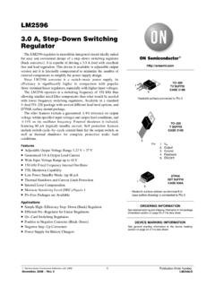
10 This is a stress rating only; functional operation of the product at these or any other conditions above those indicated in the operational section of this specification is not implied. Operation beyond the maximum operating conditions for extended periods may affect product reliability. ESD CAUTION Data Sheet AD8307 Rev. E | Page 5 of 24 PIN CONFIGURATION AND FUNCTION DESCRIPTIONS INPVPSENBINTCOMOFSOUTINMAD8307 TOP VIEW(Not to Scale)1234876501082-002 Figure 2. Pin Configuration Table 4. Pin Function Descriptions Pin No. Mnemonic Description 1 INM Signal Input Minus Polarity. Normally at VPOS/2. 2 COM Common Pin (Usually Grounded). 3 OFS Offset Adjustment. External capacitor connection. 4 OUT Logarithmic (RSSI) Output Voltage.