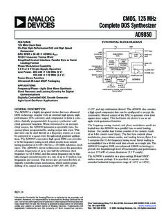
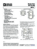
Transcription of Low Cost Micropower, Low Noise CMOS Rail-to …
1 Low Cost micropower , Low Noise cmos . Rail-to - rail , input / output operational Amplifiers data sheet ad8613 /AD8617/AD8619. FEATURES PIN CONFIGURATIONS. Offset voltage: mV maximum Low input bias current: 1 pA maximum OUT 1 ad8613 5 V+. V 2 TOP VIEW. 05622-037. Single-supply operation: V to V (Not to Scale). +IN 3 4 IN. Low Noise : 22 nV/ Hz micropower : 50 A/ amplifier maximum over temperature Figure 1. 5-Lead SC70 and 5-Lead TSOT-23. No phase reversal Unity gain stable OUT A 1 8 V+. IN A 2 AD8617 7 OUT B. Qualified for automotive applications TOP VIEW. +IN A 3 6 IN B. (Not to Scale). 05622-001. APPLICATIONS V 4 5 +IN B. Battery-powered instrumentation Figure 2.
2 8-Lead MSOP and 8-Lead SOIC_N. Multipole filters Current shunt sense OUT A 1 8 V+. Sensors IN A 2 AD8617 7 OUT B. ADC predrivers TOP VIEW. +IN A 3 6 IN B. (Not to Scale). DAC drivers/level shifters V 4 5 +IN B. Low power ASIC input or output amplifiers NOTES. 05622-002. GENERAL DESCRIPTION 1. PIN 4 AND THE EXPOSED PAD. MUST BE CONNECTED TO V . The ad8613 /AD8617/AD8619 are single, dual, and quad micro- Figure 3. 8-Lead LFCSP. power, Rail-to - rail input and output amplifiers that feature low supply current, as well as low input voltage and current Noise . OUT A 1 14 OUT D. The parts are fully specified to operate from V to 5 V single IN A 2 13 IN D. supply, or V and V dual supply.
3 The combination of low +IN A 3 AD8619 12 +IN D. TOP VIEW. Noise , very low input bias currents, and low power consumption V+ 4. (Not to Scale). 11 V . make the ad8613 /AD8617/AD8619 especially useful in portable +IN B 5 10 +IN C. and loop-powered instrumentation. IN B 6 9 IN C. 05622-035. OUT B 7 8 OUT C. The ability to swing Rail-to - rail at both the input and output enables designers to buffer cmos ADCs, DACs, ASICs, and Figure 4. 14-Lead TSSOP and 14-Lead SOIC. other wide output swing devices in low power, single-supply systems. The ad8613 is available in a 5-lead SC70 package and a 5-lead TSOT-23 package. The AD8617 is available in 8-lead MSOP, 8-lead SOIC, and 8-lead LFCSP packages.
4 The AD8619 is available in 14-lead TSSOP and 14-lead SOIC packages. The AD8617W is qualified for automotive applications and is available in 8-lead MSOP and 8-lead SOIC packages. The AD8619W is qualified for automotive applications and is available in 14-lead SOIC and 14-lead TSSOP packages. Rev. H Document Feedback Information furnished by analog devices is believed to be accurate and reliable. However, no responsibility is assumed by analog devices for its use, nor for any infringements of patents or other rights of third parties that may result from its use. Specifications subject to change without notice. No One Technology Way, Box 9106, Norwood, MA 02062-9106, license is granted by implication or otherwise under any patent or patent rights of analog devices .
5 Tel: 2005 2016 analog devices , Inc. All rights reserved. Trademarks and registered trademarks are the property of their respective owners. Technical Support ad8613 /AD8617/AD8619 data sheet TABLE OF CONTENTS. Features .. 1 Thermal Resistance ..5. Applications .. 1 ESD General Description .. 1 Typical Performance Characteristics ..6. Pin Configurations .. 1 Outline Dimensions .. 12. Revision History .. 2 Ordering Guide .. 15. 3 Automotive Products .. 16. Absolute Maximum 5. REVISION HISTORY. 5/2016 Rev. G to Rev. H Changes to input Characteristics, input Voltage Range Parameter;. Changed CP-8-9 to CP-8-21 .. Throughout Dynamic Performance, Settling Time to and Phase Margin Changed LFCSP_VD to LFCSP.
6 Throughout Parameters; and Noise Performance, Peak-to-Peak Noise Changes to Figure 3 .. 1 Parameter, Table 1 ..3. Changes to Table 4 .. 5 Changes to input Characteristics, input Voltage Range Parameter;. Changes to Figure 43 .. 15 Dynamic Performance, Settling Time to and Phase Margin Updated Outline Dimensions .. 15 Parameters; and Noise Performance, Peak-to-Peak Noise Changes to Ordering Guide .. 15 Parameter, Table 2 ..4. Changes to Table 3 and Table 4 ..5. 12/2014 Rev. F to Rev. G Changes to Figure 12 to Figure 15 ..7. Changes to General Description Section .. 1 Changes to Figure 18 Caption ..8. Changes to Ordering Guide .. 15 Changes to Figure 30 and Figure 31.
7 10. Updated Outline Dimensions .. 12. 4/2014 Rev. E to Rev. F Added Figure 44; Renumbered Sequentially .. 14. Changes to General Description Section .. 1 Changes to Ordering Guide .. 15. Changes to Table 3 .. 5. Changes to Ordering Guide .. 15 1/2006 Rev. A to Rev. B. Added Automotive Products Section .. 15 Added ad8613 .. Universal Changes to Features ..1. 3/2010 Rev. D to Rev. E Changes to Table Changes to General Description .. 1 Changes to Table Changes to Ordering Guide .. 15 Updated Outline Dimensions .. 12. Changes to Ordering Guide .. 13. 3/2010 Rev. C to Rev. D. Changes to General Description .. 1 10/2005 Rev. 0 to Rev. A. Changes to Ordering Guide.
8 15 Added AD8619 .. Universal Change to Specifications Section ..3. 10/2009 Rev. B to Rev. C Updated Outline Dimensions .. 12. Added 8-Lead LFCSP Package .. Universal Changes to Ordering Guide .. 13. Changes to Features Section, Figure 2 Caption, General Description Section, and Figure 3 .. 1 9/2005 Revision 0: Initial Version Changed VS to VSY Throughout .. 3. Rev. H | Page 2 of 16. data sheet ad8613 /AD8617/AD8619. SPECIFICATIONS. Electrical characteristics at VSY = 5 V, VCM = VSY/2, TA = 25 C, unless otherwise noted. Table 1. Parameter Symbol Conditions Min Typ Max Unit input CHARACTERISTICS. Offset Voltage VOS V < VCM < + V mV. 40 C < TA < +125 C, V < VCM < + V mV.
9 Offset Voltage Drift VOS/ T 40 C < TA < +125 C 1 V/ C. ad8613 V/ C. input Bias Current IB 1 pA. 40 C < TA < +85 C 110 pA. 40 C < TA < +125 C 780 pA. input Offset Current IOS pA. 40 C < TA < +85 C 50 pA. 40 C < TA < +125 C 250 pA. input Voltage Range IVR 0 5 V. Common-Mode Rejection Ratio CMRR 0 V < VCM < 5 V 95 dB. 40 C < TA < +125 C 68 dB. Large Signal Voltage Gain AVO RL = 10 k , V < VO < V 235 500 V/mV. input Capacitance CDIFF pF. CCM pF. output CHARACTERISTICS. output Voltage High VOH IL = 1 mA V. 40 C to +125 C V. IL = 10 mA V. 40 C to +125 C V. output Voltage Low VOL IL = 1 mA 20 30 mV. 40 C to +125 C 50 mV. IL = 10 mA 190 275 mV. 40 C to +125 C 335 mV.
10 Short-Circuit Current ISC 80 mA. Closed-Loop output Impedance ZOUT f = 10 kHz, AV = 1 15 . POWER SUPPLY. Power Supply Rejection Ratio PSRR V < VSY < 5 V 67 94 dB. 40 C < TA < +125 C 64 dB. Supply Current/ amplifier ISY VO = VSY/2 38 A. 40 C <TA < +125 C 50 A. DYNAMIC PERFORMANCE. Slew Rate SR RL = 10 k V/ s Settling Time to tS G = 1, VIN = 2 V step, CL = 20 pF, RL = 1 k 23 s Gain Bandwidth Product GBP RL = 100 k 400 kHz RL = 10 k 350 kHz Phase Margin M RL = 10 k , RL = 100 k , CL = 20 pF 70 Degrees Noise PERFORMANCE. Peak-to-Peak Noise en p-p Hz to 10 Hz V. Voltage Noise Density en f = 1 kHz 25 nV/ Hz f = 10 kHz 22 nV/ Hz Current Noise Density in f = 1 kHz pA/ Hz Rev.
