Transcription of Low-noise JFET quad operational amplifier
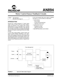
1 This is information on a product in full production. November 2013 DocID2297 Rev 51/18TL074 Low-noise jfet quad operational amplifier Datasheet - production dataFeatures Wide common-mode (up to VCC+) and differential voltage range Low input bias and offset current Low noise en = 15 nV/ Hz (typ) Output short-circuit protection high input impedance jfet input stage Low harmonic distortion: (typical) Internal frequency compensation Latch up free operation high slew rate: 16 V/ s (typical)Related products See TL071 for single version See TL072 for dual versionDescriptionThe TL074, TL074A, and TL074B are high -speed jfet input single operational amplifiers. Each of these jfet input operational amplifiers incorporates well matched, high -voltage jfet and bipolar transistors in a monolithic integrated devices feature high slew rates, low input bias and offset currents, and low offset voltage temperature Input 2 Non-inverting Input 2 Non-inverting Input 1 CCV -CCV1234856791011121314+Output 3 Output 4 Non-inverting Input 4 Inverting Input 4 Non-inverting Input 3 Inverting Input 3-+-+-+-+Output 1 Inverting Input 1 Output 2 DSO14(plastic micropackage)Pin connections(top view) Rev 5 Contents1 Schematic diagram.
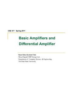
2 32 Absolute maximum ratings and operating conditions .. 43 Electrical characteristics .. 54 Parameter measurement information .. 105 Typical applications .. 116 Package information .. package information .. 147 Ordering information .. 168 Revision history .. 17 DocID2297 Rev 53/18TL074 Schematic diagram181 Schematic diagramFigure 1. Circuit schematicOutputNon-invertinginputInverti nginputVCCVCC200 100 TL074 Absolute maximum ratings and operating conditionsTL0744/18 DocID2297 Rev 52 Absolute maximum ratings and operating conditions Table 1. Absolute maximum ratingsSymbolParameterValueUnitTL074I, AI, BITL074C, AC, BCVCCS upply voltage (1) 18 VViInput voltage(2) 15 VidDifferential input voltage(3) 30 PtotPower dissipation680mWRthjaThermal resistance junction to ambient(4)(5) SO14105 C/WRthjcThermal resistance junction to case(4)(5) SO1431 Output short-circuit duration(6)InfiniteToperOperating free-air temperature range-40 to +1250 to +70 CTstgStorage temperature range-65 to +150 ESDHBM: human body model(7)1kVMM: machine model(8)200 VCDM.
3 Charged device model(9) All voltage values, except differential voltage, are with respect to the zero reference level (ground) of the supply voltages where the zero reference level is the midpoint between VCC+ and The magnitude of the input voltage must never exceed the magnitude of the supply voltage or 15 volts, whichever is differential voltages are the non-inverting input terminal with respect to the inverting input Short-circuits can cause excessive heating. Destructive dissipation can result from simultaneous short-circuits on all Rth are typical The output may be shorted to ground or to either supply. Temperature and/or supply voltages must be limited to ensure that the dissipation rating is not Human body model: 100pF discharged through a resistor between two pins of the device, done for all couples of pin combinations with other pins Machine model: a 200pF cap is charged to the specified voltage, then discharged directly between two pins of the device with no external series resistor (internal resistor < 5 ), done for all couples of pin combinations with other pins Charged device model: all pins plus package are charged together to the specified voltage and then discharged directly to the 2.
4 Operating conditionsSymbolParameterTL074I, AI, BITL074C, AC, BCUnitVCCS upply voltage6 to 36 VToperOperating free-air temperature range-40 to +1250 to +70 CDocID2297 Rev 55/18TL074 Electrical characteristics183 Electrical characteristics Table 3. VCC = 15 V, Tamb = +25 C (unless otherwise specified) SymbolParameterTL074I,AC,AI, BC, offset voltage (Rs = 50 ) Tamb = +25 C TL074 TL074A TL074B Tmin Tamb TmaxTL074 TL074A TL074B3311063137531013mVDVioInput offset voltage drift1010 V/ CIioInput offset current Tamb = +25 C Tmin Tamb Tmax51004510010pAnAIibInput bias current -note (1)Tamb = +25 C Tmin Tamb Tmax20200203020020pAnAAvdLarge signal voltage gain RL= 2k , Vo= 10 VTamb = +25 C Tmin Tamb Tmax50252002515200V/mVSVRS upply voltage rejection ratio (RS = 50 )
5 Tamb = +25 C Tmin Tamb Tmax808086707086dBICCS upply current, no load Tamb = +25 C Tmin Tamb common mode voltage range 11+15-12 11+15-12 VCMRC ommon mode rejection ratio (RS = 50 )Tamb = +25 C Tmin Tamb Tmax808086707086dBIosOutput short-circuit currentTamb = +25 C Tmin Tamb Tmax10104060601010406060mA VoppOutput voltage swing Tamb = +25 C RL = 2k RL = 10k Tmin Tamb Tmax RL = 2k RL = 10k rateVin = 10V, RL = 2k , CL = 100pF, unity gain813813V/ sElectrical characteristicsTL0746/18 DocID2297 Rev 5trRise timeVin = 20mV, RL = 2k , CL = 100pF, unity sKovOvershootVin = 20mV, RL = 2k , CL = 100pF, unity gain1010%GBPGain bandwidth productVin= 10mV, RL= 2k , CL = 100pF, = 100kHz2323 MHzRiInput resistance10121012 THDT otal harmonic distortion f= 1kHz, RL = 2k ,CL = 100pF, Av = 20dB, Vo = 2 Vpp)
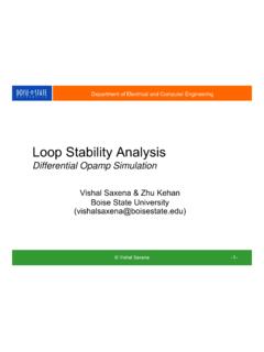
6 Input noise voltageRS = 100 , f = 1kHz1515 mPhase margin4545degreesVo1/Vo2 Channel separation Av = 100120120dB1. The input bias currents are junction leakage currents which approximately double for every 10 C increase in the junction 3. VCC = 15 V, Tamb = +25 C (unless otherwise specified) (continued)SymbolParameterTL074I,AC,AI, BC, Rev 57/18TL074 Electrical characteristics18 Figure 2. Maximum peak-to-peak output voltage versus frequencyFigure 3. Maximum peak-to-peak output voltage versus frequency Figure 4. Maximum peak-to-peak output voltage versus frequencyFigure 5. Maximum peak-to-peak output voltage versus free air temperature Figure 6.
7 Maximum peak-to-peak output voltage versus load resistanceFigure 7. Maximum peak-to-peak output voltage versus supply voltage 302520151050246810121416 MAXIMUM PE AK-TO-PEAK OUTPUTVOLTAG E (V)RL= 10 k Tamb= +25 CSUPPLY VOLTAGE ( V)Electrical characteristicsTL0748/18 DocID2297 Rev 5 Figure 8. Input bias current versus free air temperatureFigure 9. Large signal differential voltage amplification versus free air temperature 302520151050246810121416 MAXIMUM PE AK-TO-PEAK OUTPUTVOLTAG E (V)RL= 10 k Tamb= +25 CSUPPLY VOLTAGE ( V)1000400200100204010421 differential VOLTAGE AMPLIFICATION (V/mV)-75-50-250255075100125 TEMPERATURE ( C)RL= 2k VO= 10 VVCC= 15 VFigure 10.
8 Large signal differential voltage amplification and phase shift versus frequencyFigure 11. Total power dissipation versus free air temperature (V/mV)2502252001751501251007550250 TOTAL POW E R DIS S IPATION (mW)-75-50-250255075100125 TEMPERATURE ( C )VCC= 15 VNo signalNo loadFigure 12. Supply current per amplifier versus free air temperatureFigure 13. Common mode rejection ratio versus free air temperature CURRENT (mA)-75-50-250255075100125 TEMPERATURE ( C )VCC= 15 VNo signalNo load898887868584-50-25 0 2550 75100125C OMMO N MODE MOD E R E J E C T IO NRATIO (dB)TEMPERATURE ( C )83-75RL= 1 0 k = 15 VVCCDocID2297 Rev 59/18TL074 Electrical characteristics18 Figure 14.
9 Voltage follower large signal pulse responseFigure 15. Output voltage versus elapsed time tr2824201612840-4 OUTPUT VOLTAGE (mV) ( s)10%90%OVERSHOOTRL= 2k Tamb= +25 CVCC= 15 VFigure 16. Equivalent input noise voltage versus frequencyFigure 17. Total harmonic distortion versus frequency 706050403020100E Q UIVAL E NT INP UT NO IS EVOLTAGE (nV/VHz)10401004001k4k10k40k 100kFREQUENCY (Hz)AV= 10RS= 100 Tamb= +25 CVCC= HARMONIC DISTORTION(% )1004001k4k10k40k100kFREQUENCY (Hz)AV= 1 Tamb= +25 CVCC= 15V= 6 VVO(rms)AV= 1 Tamb= +25 C= 6 VVO(rms)VCC= 15 VParameter measurement informationTL07410/18 DocID2297 Rev 54 Parameter measurement information Figure 18.
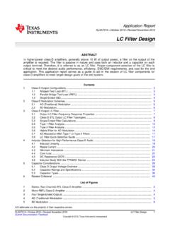
10 Voltage followerFigure 19. Gain-of-10 inverting amplifier -eITL074RL1/4CL= 100pF1k 10k eoDocID2297 Rev 511/18TL074 Typical applications185 Typical applicationsFigure 20. Audio distribution amplifierFigure 21. Positive feeback bandpass filter-TL0741/4---TL0741/4TL0741/4TL0741 /41M 1 FOutput AOutput BOutput CInput100k 100k 100k 100k 1OO FVCC+f = 100kHzO--TL0741/4220pF43k 43k 220pF43 k 16k TL0741/430k Output A-TL0741 220pF43k 220pF43 k -TL0741/443k 16k 30k Output BGroundTypical applicationsTL07412/18 DocID2297 Rev 5 Figure 22. Output AFigure 23. Output BSECOND ORDER BANDPASS FILTER fo = 100 kHz; Q = 30; Gain = 16 CASCADED BANDPASS FILTER fo = 100 kHz; Q = 69; Gain = 16 DocID2297 Rev 513/18TL074 Package information186 Package informationIn order to meet environmental requirements, ST offers these devices in different grades of ECOPACK packages, depending on their level of environmental compliance.