Transcription of Low Noise Precision Difet® Operational Amplifier
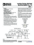
1 opa111 . Low Noise Precision Difet . Operational Amplifier . FEATURES APPLICATIONS. LOW Noise : 100% Tested, 8nV Hz max Precision INSTRUMENTATION. (10kHz) DATA ACQUISITION. LOW BIAS CURRENT: 1pA max TEST EQUIPMENT. LOW OFFSET: 250 V max OPTOELECTRONICS. LOW DRIFT: 1 V/ C max MEDICAL EQUIPMENT CAT SCANNER. HIGH OPEN-LOOP GAIN: 120dB min RADIATION HARD EQUIPMENT. HIGH COMMON-MODE REJECTION: 100dB min DESCRIPTION. The opa111 is a Precision monolithic dielectrically Case and +VCC. isolated FET (Difet ) Operational Amplifier . Outstand- Substrate ing performance characteristics allow its use in the 8 7.
2 Most critical instrumentation applications. In Noise , bias current, voltage offset, drift, open-loop 2. gain, common-mode rejection, and power supply re- +In jection are superior to BIFET amplifiers. 3. Noise -Free Cascode*. Very low bias current is obtained by dielectric isola- tion with on-chip guarding. Output Laser trimming of thin-film resistors gives very low 6. offset and drift. Extremely low Noise is achieved with 2k . 2k . patented circuit design techniques. A new cascode Trim 10k . design allows high Precision input specifications and 1. reduced susceptibility to flicker Noise .
3 Trim 10k . Standard 741 pin configuration allows upgrading of 5. 2k 2k VCC. existing designs to higher performance levels. *Patented 4. BIFET National Semiconductor Corp., Difet Burr-Brown Corp. International Airport Industrial Park Mailing Address: PO Box 11400 Tucson, AZ 85734 Street Address: 6730 S. Tucson Blvd. Tucson, AZ 85706. Tel: (520) 746-1111 Twx: 910-952-1111 Cable: BBRCORP Telex: 066-6491 FAX: (520) 889-1510 Immediate Product Info: (800) 548-6132. 1984 Burr-Brown Corporation PDS-526K Printed in August, 1995. SBOS138. SPECIFICATIONS. ELECTRICAL. At VCC = 15 VDC and TA = +25 C unless otherwise noted.
4 opa111am OPA111BM OPA111SM. PARAMETER CONDITION MIN TYP MAX MIN TYP MAX MIN TYP MAX UNITS. INPUT. Noise . Voltage, fO = 10Hz 100% Tested 40 80 30 60 40 80 nV/ Hz fO = 100Hz 100% Tested 15 40 11 30 15 40 nV/ Hz fO = 1kHz 100% Tested 8 15 7 12 8 15 nV/ Hz fO = 10kHz 100% Tested 6 8 6 8 6 8 nV/ Hz fB = 10Hz to 10kHz 100% Tested 1 Vrms fB = to 10Hz (1) Vp-p Current, fB = to 10Hz (1) 15 12 15 fAp-p fO = thru 20kHz (1) fA/ Hz OFFSET VOLTAGE(2). Input Offset Voltage VCM = 0 VDC 100 500 50 250 100 500 V. Average Drift TA = TMIN to TMAX 2 5 1 2 5 V/ C. Supply Rejection VCC = 10V to 18V 90 110 100 110 90 110 dB.
5 3 31 3 10 3 31 V/V. BIAS CURRENT(2). Input Bias Current VCM = 0 VDC 2 1 2 pA. OFFSET CURRENT(2). Input Offset Current VCM = 0 VDC pA. IMPEDANCE. Differential 1013 || 1 1013 || 1 1013 || 1 || pF. Common-Mode 1014 || 3 1014 || 3 1014 || 3 || pF. VOLTAGE RANGE. Common-Mode Input Range 10 11 10 11 10 11 V. Common-Mode Rejection VIN = 10 VDC 90 110 100 110 90 110 dB. OPEN-LOOP GAIN, DC. Open-Loop Voltage Gain RL 2k 114 125 120 125 114 125 dB. FREQUENCY RESPONSE. Unity Gain, Small Signal 2 2 2 MHz Full Power Response 20Vp-p, RL = 2k 16 32 16 32 16 32 kHz Slew Rate VO = 10V, RL = 2k 1 2 1 2 1 2 V/ s Settling Time, Gain = 1, RL = 2k 6 6 6 s 10V Step 10 10 10 s Overload Recovery, 50% Overdrive(3) Gain = 1 5 5 5 s RATED OUTPUT.
6 Voltage Output RL = 2k 11 12 11 12 11 12 V. Current Output VO = 10 VDC 10 10 10 mA. Output Resistance DC, Open Loop 100 100 100 . Load Capacitance Stability Gain = +1 1000 1000 1000 pF. Short Circuit Current 10 40 10 40 10 40 mA. POWER SUPPLY. Rated Voltage 15 15 15 VDC. Voltage Range, Derated Performance 5 18 5 18 5 18 VDC. Current, Quiescent IO = 0mADC mA. TEMPERATURE RANGE. Specification Ambient Temp. 25 +85 25 +85 55 +125 C. Operating Ambient Temp. 55 +125 55 +125 55 +125 C. Storage Ambient Temp. 65 +150 65 +150 65 +150 C. Junction-Ambient 200 200 200 C/W. NOTES: (1) Sample tested this parameter is guaranteed.
7 (2) Offset voltage, offset current, and bias current are measured with the units fully warmed up. (3) Overload recovery is defined as the time required for the output to return from saturation to linear operation following the removal of a 50% input overdrive. The information provided herein is believed to be reliable; however, BURR-BROWN assumes no responsibility for inaccuracies or omissions. BURR-BROWN assumes no responsibility for the use of this information, and all use of such information shall be entirely at the user's own risk. Prices and specifications are subject to change without notice.
8 No patent rights or licenses to any of the circuits described herein are implied or granted to any third party. BURR-BROWN does not authorize or warrant any BURR- BROWN product for use in life support devices and/or systems.. opa111 2. ELECTRICAL (FULL TEMPERATURE RANGE SPECIFICATIONS). At VCC = 15 VDC and TA = TMIN to TMAX unless otherwise noted. opa111am OPA111BM OPA111SM. PARAMETER CONDITION MIN TYP MAX MIN TYP MAX MIN TYP MAX UNITS. TEMPERATURE RANGE. Specification Range Ambient Temp. 25 +85 25 +85 55 +125 C. INPUT. OFFSET VOLTAGE(1). Input Offset Voltage VCM = 0 VDC 220 1000 110 500 300 1500 V.
9 Average Drift 2 5 1 2 5 V/ C. Supply Rejection VCC = 10V to 18V 86 100 90 100 86 100 dB. 10 50 10 32 10 50 V/V. BIAS CURRENT(1). Input Bias Current VCM = 0 VDC 50 250 30 130 820 4100 pA. OFFSET CURRENT(1). Input Offset Current VCM = 0 VDC 30 200 15 100 510 3100 pA. VOLTAGE RANGE. Common-Mode Input Range 10 11 10 11 10 11 V. Common-Mode Rejection VIN = 10 VDC 86 100 90 100 86 100 dB. OPEN-LOOP GAIN, DC. Open-Loop Voltage Gain RL 2k 110 120 114 120 110 120 dB. RATED OUTPUT. Voltage Output RL = 2k 11 11 11 V. Current Output VO = 10 VDC 10 10 10 mA. Short Circuit Current VO = 0 VDC 10 40 10 40 10 40 mA.
10 POWER SUPPLY. Current, Quiescent IO = 0mADC mA. NOTES: (1) Offset voltage, offset current, and bias current are measured with the units fully warmed up. CONNECTION DIAGRAM ABSOLUTE MAXIMUM RATINGS. Top View Substrate and Case Supply .. 18 VDC. Internal Power Dissipation(1) .. 750mW. 8 Differential Input Voltage(2) .. 36 VDC. Offset Trim 1 7 +VCC Input Voltage Range(2) .. 18 VDC. Storage Temperature Range .. 65 C to +150 C. Operating Temperature Range .. 55 C to +125 C. In 2 opa111 6 Output Lead Temperature (soldering, 10s) .. +300 C. Output Short Circuit Duration(3).