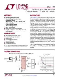
Transcription of LT3042 - 20V, 200mA, Ultralow Noise, Ultrahigh PSRR RF ...
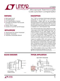
1 LT304213042fbFor more information APPLICATION FEATURESDESCRIPTION20V, 200ma , Ultralow noise , Ultrahigh PSRR RF linear RegulatorThe LT 3042 is a high performance low dropout linear regulator featuring LTC s Ultralow noise and Ultrahigh PSRR architecture for powering noise sensitive RF applications. Designed as a precision current reference followed by a high performance voltage buffer, the LT3042 can be easily paralleled to further reduce noise , increase output current and spread heat on the device supplies 200ma at a typical 350mV dropout voltage. Operating quiescent current is nominally 2mA and drops to <<1 A in shutdown. The LT3042 s wide output voltage range (0V to 15V) while maintaining unity-gain operation provides virtually constant output noise , PSRR, bandwidth and load regulation, independent of the programmed output voltage. Additionally, the regulator features programmable current limit, fast start-up capa-bility and programmable power good to indicate output voltage LT3042 is stable with a minimum F ceramic output capacitor.
2 Built-in protection includes reverse bat-tery protection, reverse current protection, internal current limit with foldback and thermal limit with hysteresis. The LT3042 is available in thermally enhanced 10-Lead MSOP and 3mm 3mm DFN Supply Ripple RejectionAPPLICATIONS nUltralow RMS noise : VRMS (10Hz to 100kHz) nUltralow Spot noise : 2nV/ Hz at 10kHz nUltrahigh PSRR: 79dB at 1 MHz nOutput Current: 200ma nWide Input Voltage Range: to 20V nSingle Capacitor Improves noise and PSRR n100 A SET Pin Current: 1% Initial Accuracy nSingle Resistor Programs Output Voltage nHigh Bandwidth: 1 MHz nProgrammable Current Limit nLow Dropout Voltage: 350mV nOutput Voltage Range: 0V to 15V nProgrammable Power Good nFast Start-Up Capability nPrecision Enable/UVLO nParallelable for Lower noise and Higher Current nInternal Current Limit with Foldback nMinimum Output Capacitor: F Ceramic nReverse Battery and Reverse Current Protection n10-Lead MSOP and 3mm 3mm DFN Packages nRF Power Supplies: PLLs, VCOs, Mixers, LNAs nVery Low noise Instrumentation nHigh Speed/High Precision Data Converters nMedical Applications.
3 Imaging, Diagnostics nPrecision Power Supplies nPost-Regulator for Switching SuppliesAll registered trademarks and trademarks are the property of their respective owners. Patents Pending. FREQUENCY (Hz)40 PSRR (dB)80120601001010010k100k1M10M3042 TA01b201k30701105090 VIN = 5 VRSET = CSET = FCOUT = FIL = 200ma + 100 AINEN/UVPGGNDOUTLT3042 ILIMPGFB453k1% FVIN5V 5% (MAX) TA01a499 more information CONFIGURATIONABSOLUTE MAXIMUM RATINGSIN Pin Voltage .. 22 VEN/UV Pin Voltage .. 22 VIN-to-EN/UV 22 VPG Pin Voltage (Note 10) .. , 22 VILIM Pin Voltage (Note 10) .. , 1 VPGFB Pin Voltage (Note 10) .. , 22 VSET Pin Voltage (Note 10) .. , 16 VSET Pin Current (Note 7) .. 20mAOUTS Pin Voltage (Note 10) .. , 16 VOUTS Pin Current (Note 7) .. 20mAOUT Pin Voltage (Note 10) .. , 16V(Note 1)TOP VIEW11 GNDDD PACKAGE10-LEAD (3mm 3mm) PLASTIC DFN10967845321 OUTOUTSGNDSETPGFBININEN/UVPGILIM TJMAX = 150 C, JA = 34 C/W, JC = C/W EXPOSED PAD (PIN 11) IS GND, MUST BE SOLDERED TO PCB12345 ININEN/UVPGILIM109876 OUTOUTSGNDSETPGFBTOP VIEW11 GNDMSE PACKAGE10-LEAD PLASTIC MSOP TJMAX = 150 C, JA = 33 C/W, JC = 8 C/W EXPOSED PAD (PIN 11) IS GND, MUST BE SOLDERED TO PCBORDER INFORMATIONLEAD FREE FINISHTAPE AND REELPART MARKING*PACKAGE DESCRIPTIONTEMPERATURE RANGELT3042 EDD#PBFLT3042 EDD#TRPBFLGSJ10-Lead (3mm 3mm) Plastic DFN 40 C to 125 CLT3042 IDD#PBFLT3042 IDD#TRPBFLGSJ10-Lead (3mm 3mm) Plastic DFN 40 C to 125 CLT3042 HDD#PBFLT3042 HDD#TRPBFLGSJ10-Lead (3mm 3mm) Plastic DFN 40 C to 150 CLT3042 MPDD#PBFLT3042 MPDD#TRPBFLGSJ10-Lead (3mm 3mm)
4 Plastic DFN 55 C to 150 CLT3042 EMSE#PBFLT3042 EMSE#TRPBFLTGSH10-Lead Plastic MSOP 40 C to 125 CLT3042 IMSE#PBFLT3042 IMSE#TRPBFLTGSH10-Lead Plastic MSOP 40 C to 125 CLT3042 HMSE#PBFLT3042 HMSE#TRPBFLTGSH10-Lead Plastic MSOP 40 C to 150 CLT3042 MPMSE#PBFLT3042 MPMSE#TRPBFLTGSH10-Lead Plastic MSOP 55 C to 150 CConsult ADI Marketing for parts specified with wider operating temperature ranges. *The temperature grade is identified by a label on the shipping ADI Marketing for information on nonstandard lead based finish more information on lead free part marking, go to: For more information on tape and reel specifications, go to: Some packages are available in 500 unit reels through designated sales channels with #TRMPBF Differential (Note 14) .. Differential .. 22 VIN-to-OUTS Differential .. 22 VOutput Short-Circuit Duration ..IndefiniteOperating Junction Temperature Range (Note 9) E-, I-Grade .. 40 C to 125 C H-Grade .. 40 C to 150 C MP-Grade .. 55 C to 150 CStorage Temperature Range.
5 65 C to 150 CLead Temperature (Soldering, 10 Sec) MSE Package ..300 #orderinfoLT304233042fbFor more information CHARACTERISTICS The l denotes the specifications which apply over the full operating temperature range, otherwise specifications are at TA = 25 IN Pin Voltage (Note 2)ILOAD = 200ma , VIN UVLO Rising VIN UVLO 752V mVSET Pin Current (ISET)VIN = 2V, ILOAD = 1mA, VOUT = 2V < VIN < 20V, 0V < VOUT < 15V, 1mA < ILOAD < 200ma (Note 3) l99 98100 100101 102 A AFast Start-Up Set Pin CurrentVPGFB = 289mV, VIN = , VSET = Offset Voltage VOS (VOUT VSET) (Note 4)VIN = 2V, ILOAD = 1mA, VOUT = 2V < VIN < 20V, 0V < VOUT < 15V, 1mA < ILOAD < 200ma (Note 3) l 1 21 2mV mVLine Regulation: ISET Line Regulation: VOSVIN = 2V to 20V, ILOAD = 1mA, VOUT = VIN = 2V to 20V, ILOAD = 1mA, VOUT = (Note 4)l 2 3nA/V V/VLoad Regulation.
6 ISET Load Regulation: VOSILOAD = 1mA to 200ma , VIN = 2V, VOUT = ILOAD = 1mA to 200ma , VIN = 2V, VOUT = (Note 4) l3 mVChange in ISET with VSET Change in VOS with VSET Change in ISET with VSET Change in VOS with VSETVSET = to 15V, VIN = 20V, ILOAD = 1mA VSET = to 15V, VIN = 20V, ILOAD = 1mA (Note 4) VSET = 0V to , VIN = 20V, ILOAD = 1mA VSET = 0V to , VIN = 20V, ILOAD = 1mA (Note 4)l l l l30 150 600 2nA mV nA mVDropout VoltageILOAD = 1mA, 50mA l220270 300mV mVILOAD = 150mA (Note 5)270mVILOAD = 200ma (Note 5)350mVGND Pin Current VIN = VOUT(NOMINAL) (Note 6)ILOAD = 10 A ILOAD = 1mA ILOAD = 50mA ILOAD = 100mA ILOAD = 200ma l l l 2 5 7 13mA mA mA mA mAOutput noise Spectral Density (Notes 4, 8)ILOAD = 200ma , Frequency = 10Hz, COUT = F, CSET = F, VOUT = ILOAD = 200ma , Frequency = 10Hz, COUT = F, CSET = F, VOUT 15V ILOAD = 200ma , Frequency = 10kHz, COUT = F, CSET = F, VOUT 15V ILOAD = 200ma , Frequency = 10kHz, COUT = F, CSET = F, 0V VOUT < 60 2 5nV/ Hz nV/ Hz nV/ Hz nV/ HzOutput RMS noise (Notes 4, 8)ILOAD = 200ma , BW = 10Hz to 100kHz, COUT = F, CSET = F, VOUT = ILOAD = 200ma , BW = 10Hz to 100kHz, COUT = F, CSET = F, VOUT 15V ILOAD = 200ma , BW = 10Hz to 100kHz, COUT = F, CSET = F, 0V VOUT < VRMS VRMS VRMSR eference Current RMS Output noise (Notes 4, 8)BW = 10Hz to 100kHz6nARMSR ipple Rejection VOUT 15V VIN VOUT = 2V (Avg) (Notes 4, 15)
7 VRIPPLE = 500mVP-P, fRIPPLE = 120Hz, ILOAD = 200ma , COUT = F, CSET = F VRIPPLE = 150mVP-P, fRIPPLE = 10kHz, ILOAD = 200ma , COUT = F, CSET = F VRIPPLE = 150mVP-P, fRIPPLE = 100kHz, ILOAD = 200ma , COUT = F, CSET = F VRIPPLE = 150mVP-P, fRIPPLE = 1 MHz, ILOAD = 200ma , COUT = F, CSET = F VRIPPLE = 80mVP-P, fRIPPLE = 10 MHz, ILOAD = 200ma , COUT = F, CSET = F95117 91 78 79 56dB dB dB dB dBRipple Rejection 0V VOUT < VIN VOUT = 2V (Avg) (Notes 4, 8)VRIPPLE = 500mVP-P, fRIPPLE = 120Hz, ILOAD = 200ma , COUT = F, CSET = F VRIPPLE = 50mVP-P, fRIPPLE = 10kHz, ILOAD = 200ma , COUT = F, CSET = F VRIPPLE = 50mVP-P, fRIPPLE = 100kHz, ILOAD = 200ma , COUT = F, CSET = F VRIPPLE = 50mVP-P, fRIPPLE = 1 MHz, ILOAD = 200ma , COUT = F, CSET = F VRIPPLE = 50mVP-P, fRIPPLE = 10 MHz, ILOAD = 200ma , COUT = F, CSET = F104 85 73 72 57dB dB dB dB dBEN/UV Pin ThresholdEN/UV Trip Point Rising (Turn-On)
8 , VIN = Pin HysteresisEN/UV Trip Point Hysteresis, VIN = 2V170mVEN/UV Pin CurrentVEN/UV = 0V, VIN = 20V VEN/UV = , VIN = 20V VEN/UV = 20V, VIN = 0Vl l 8 1 15 A A ALT304243042fbFor more information CHARACTERISTICS The l denotes the specifications which apply over the full operating temperature range, otherwise specifications are at TA = 25 Current in Shutdown (VEN/UV = 0V)VIN = 6V 10 A AInternal Current Limit (Note 12)VIN = 2V, VOUT = 0V VIN = 12V, VOUT = 0V VIN = 20V, VOUT = 0Vl l220 130270 300 180320 250mA mA mAProgrammable Current LimitProgramming Scale Factor: 2V< VIN < 20V (Note 11) VIN = 2V, VOUT = 0V, RILIM = 625 VIN = 2V, VOUT = 0V, RILIM = l l 180 45125 200 50 220 55mA k mA mAPGFB Trip PointPGFB Trip Point Risingl291300309mVPGFB HysteresisPGFB Trip Point Hysteresis7mVPGFB Pin CurrentVIN = 2V, VPGFB = 300mV25nAPG Output Low VoltageIPG = 100 Al30100mVPG Leakage CurrentVPG = 20Vl1 AReverse Input CurrentVIN = 20V, VEN/UV = 0V, VOUT = 0V, VSET = 0Vl50 AReverse Output CurrentVIN = 0, VOUT = 5V, SET = Open25 AMinimum Load Required (Note 13)VOUT < 1Vl10 AThermal ShutdownTJ Rising Hysteresis162 8 C CStart-Up TimeVOUT(NOM) = 5V, ILOAD = 200ma , CSET = F, VIN = 6V, VPGFB = 6V VOUT(NOM) = 5V, ILOAD = 200ma , CSET = F, VIN = 6V, VPGFB = 6V VOUT(NOM) = 5V, ILOAD = 200ma , CSET = F, VIN = 6V, RPG1 = 50k , RPG2 = 700k (with Fast Start-Up to 90% of VOUT)55 550 10ms ms msThermal Regulation10ms Pulse 1: Stresses beyond those listed under Absolute Maximum Ratings may cause permanent damage to the device.
9 Exposure to any Absolute Maximum Rating condition for extended periods may affect device reliability and 2: The EN/UV pin threshold must be met to ensure device 3: Maximum junction temperature limits operating conditions. The regulated output voltage specification does not apply for all possible combinations of input voltage and output current, especially due to the internal current limit foldback which starts to decrease current limit at VIN VOUT > 12V. If operating at maximum output current, limit the input voltage range. If operating at the maximum input voltage, limit the output current 4: OUTS ties directly to 5: Dropout voltage is the minimum input-to-output differential voltage needed to maintain regulation at a specified output current. The dropout voltage is measured when output is 1% out of regulation. This definition results in a higher dropout voltage compared to hard dropout which is measured when VIN = VOUT(NOMINAL). For lower output voltages, below , dropout voltage is limited by the minimum input voltage specification.
10 linear Technology is unable to guarantee maximum dropout voltage specifications at high currents due to production test limitations with Kelvin-sensing the package pins. Please consult the Typical Performance Characteristics for curves of dropout voltage as a function of output load current and temperature measured in a typical application 6: GND pin current is tested with VIN = VOUT(NOMINAL) and a current source load. Therefore, the device is tested while operating in dropout. This is the worst-case GND pin current. GND pin current decreases at higher input voltages. Note that GND pin current does not include SET pin or ILIM pin current but Quiescent current does include 7: SET and OUTS pins are clamped using diodes and two 25 series resistors. For less than 5ms transients, this clamp circuitry can carry more than the rated current. Refer to Applications Information for more 8: Adding a capacitor across the SET pin resistor decreases output voltage noise . Adding this capacitor bypasses the SET pin resistor s thermal noise as well as the reference current s noise .
