Transcription of LT3045 20V, 500mA, Ultralow Noise, Ultrahigh …
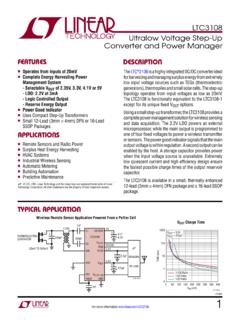
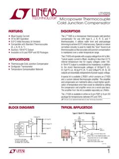
1 LT30451 Rev. BFor more information APPLICATION FEATURESDESCRIPTION20V, 500mA, Ultralow noise , Ultrahigh PSRR Linear RegulatorThe LT 3045 is a high performance low dropout linear regulator featuring LTC s Ultralow noise and Ultrahigh PSRR architecture for powering noise sensitive applica-tions. Designed as a precision current reference followed by a high performance voltage buffer, the LT3045 can be easily paralleled to further reduce noise , increase output current and spread heat on the device supplies 500mA at a typical 260mV dropout voltage. Operating quiescent current is nominally and drops to <<1 A in shutdown. The LT3045 s wide output voltage range (0V to 15V) while maintaining unity-gain operation provides virtually constant output noise , PSRR, bandwidth and load regulation, independent of the programmed output voltage.
2 Additionally, the regulator features programmable current limit, fast start-up capa-bility and programmable power good to indicate output voltage LT3045 is stable with a minimum 10 F ceramic output capacitor. Built-in protection includes reverse-battery protection, reverse-current protection, internal current limit with foldback and thermal limit with hysteresis. The LT3045 is available in thermally enhanced 12-Lead MSOP and 10-Lead 3mm 3mm DFN Supply Ripple RejectionAPPLICATIONS nUltralow RMS noise : VRMS (10Hz to 100kHz) nUltralow Spot noise : 2nV/ Hz at 10kHz nUltrahigh PSRR: 76dB at 1 MHz nOutput Current: 500mA nWide Input Voltage Range: to 20V nSingle Capacitor Improves noise and PSRR n100 A SET Pin Current: 1% Initial Accuracy nSingle Resistor Programs Output Voltage nHigh Bandwidth: 1 MHz nProgrammable Current Limit nLow Dropout Voltage: 260mV nOutput Voltage Range: 0V to 15V nProgrammable Power Good nFast Start-Up Capability nPrecision Enable/UVLO nParallelable for Lower noise and Higher Current nInternal Current Limit with Foldback nMinimum Output Capacitor.
3 10 F Ceramic nReverse-Battery and Reverse-Current Protection n12-Lead MSOP and 10-Lead 3mm 3mm DFN Packages nRF Power Supplies: PLLs, VCOs, Mixers, LNAs, PAs nVery Low noise Instrumentation nHigh Speed/High Precision Data Converters nMedical Applications: Imaging, Diagnostics nPrecision Power Supplies nPost-Regulator for Switching SuppliesAll registered trademarks and trademarks are the property of their respective = 5 VRSET = = FCOUT = 10 FIL = 500mAFREQUENCY (Hz)101001k10k100k1M10M20304050607080901 00110120 PSRR (dB)3045 TA01b+ 100 AINEN/UVPGGNDOUTLT3045 ILIMPGFB402k10 F**OPTIONAL, SEE APPLICATIONS INFORMATIONVIN5V 5% FVOUT3 VIOUT(MAX) TA01a249 FeedbackLT30452 Rev. BFor more information CONFIGURATIONABSOLUTE MAXIMUM RATINGSIN Pin Voltage .. 22 VEN/UV Pin Voltage.
4 22 VIN-to-EN/UV 22 VPG Pin Voltage (Note 10) .. , 22 VILIM Pin Voltage (Note 10) .. , 1 VPGFB Pin Voltage (Note 10) .. , 22 VSET Pin Voltage (Note 10) .. , 16 VSET Pin Current (Note 7) .. 20mAOUTS Pin Voltage (Note 10) .. , 16 VOUTS Pin Current (Note 7) .. 20mAOUT Pin Voltage (Note 10) .. , 16V(Note 1)TOP VIEW11 GNDDD PACKAGE10-LEAD (3mm 3mm) PLASTIC DFN10967845321 OUTOUTSGNDSETPGFBININEN/UVPGILIM TJMAX = 150 C, JA = 34 C/W, JC = C/W EXPOSED PAD (PIN 11) IS GND, MUST BE SOLDERED TO PCB123456 INININEN/UVPGILIM121110987 OUTOUTOUTSGNDSETPGFBTOP VIEWMSE PACKAGE12-LEAD PLASTIC MSOP13 GND TJMAX = 150 C, JA = 33 C/W, JC = 8 C/W EXPOSED PAD (PIN 13) IS GND, MUST BE SOLDERED TO PCBORDER INFORMATIONLEAD FREE FINISHTAPE AND REELPART MARKING*PACKAGE DESCRIPTIONTEMPERATURE RANGELT3045 EDD#PBFLT3045 EDD#TRPBFLGYP10-Lead (3mm 3mm) Plastic DFN 40 C to 125 CLT3045 IDD#PBFLT3045 IDD#TRPBFLGYP10-Lead (3mm 3mm) Plastic DFN 40 C to 125 CLT3045 HDD#PBFLT3045 HDD#TRPBFLGYP10-Lead (3mm 3mm)
5 Plastic DFN 40 C to 150 CLT3045 MPDD#PBFLT3045 MPDD#TRPBFLYGP10-Lead (3mm 3mm) Plastic DFN 55 C to 150 CLT3045 EMSE#PBFLT3045 EMSE#TRPBF304512-Lead Plastic MSOP 40 C to 125 CLT3045 IMSE#PBFLT3045 IMSE#TRPBF304512-Lead Plastic MSOP 40 C to 125 CLT3045 HMSE#PBFLT3045 HMSE#TRPBF304512-Lead Plastic MSOP 40 C to 150 CContact the factory for parts specified with wider operating temperature ranges. *The temperature grade is identified by a label on the shipping and reel specifications. Some packages are available in 500 unit reels through designated sales channels with #TRMPBF Differential (Note 14) .. Differential .. 22 VIN-to-OUTS Differential .. 22 VOutput Short-Circuit Duration ..IndefiniteOperating Junction Temperature Range (Note 9) E-Grade, I-Grade .. 40 C to 125 C H-Grade.
6 40 C to 150 CMP-Grade (Note 15) .. 55 C to 150 C Storage Temperature Range .. 65 C to 150 CLead Temperature (Soldering, 10 Sec) MSE Package ..300 CLT30453 Rev. BFor more information CHARACTERISTICS The l denotes the specifications which apply over the full operating temperature range, otherwise specifications are at TA = 25 Voltage Rangel220 VMinimum IN Pin Voltage (Note 2)ILOAD = 500mA, VIN UVLO Rising VIN UVLO 752V mVOutput Voltage RangeVIN > VOUTl015 VSET Pin Current (ISET)VIN = 2V, ILOAD = 1mA, VOUT = 2V < VIN < 20V, 0V < VOUT < 15V, 1mA < ILOAD < 500mA (Note 3) l99 98100 100101 102 A AFast Start-Up Set Pin CurrentVPGFB = 289mV, VIN = , VSET = Offset Voltage VOS (VOUT VSET) (Note 4)
7 VIN = 2V, ILOAD = 1mA, VOUT = 2V < VIN < 20V, 0V < VOUT < 15V, 1mA < ILOAD < 500mA (Note 3) l 1 21 2mV mVLine Regulation: ISET Line Regulation: VOSVIN = 2V to 20V, ILOAD = 1mA, VOUT = VIN = 2V to 20V, ILOAD = 1mA, VOUT = (Note 4)l 2 3nA/V V/VLoad Regulation: ISET Load Regulation: VOSILOAD = 1mA to 500mA, VIN = 2V, VOUT = ILOAD = 1mA to 500mA, VIN = 2V, VOUT = (Note 4) l3 mVChange in ISET with VSET Change in VOS with VSET Change in ISET with VSET Change in VOS with VSETVSET = to 15V, VIN = 20V, ILOAD = 1mA VSET = to 15V, VIN = 20V, ILOAD = 1mA (Note 4) VSET = 0V to , VIN = 20V, ILOAD = 1mA VSET = 0V to , VIN = 20V, ILOAD = 1mA (Note 4)l l l l30 150 600 2nA mV nA mVDropout VoltageILOAD = 1mA, 50mA l220275 330mV mVILOAD = 300mA (Note 5) l220280 350mV mVILOAD = 500mA (Note 5) l260350 450mV mVGND Pin Current VIN = VOUT(NOMINAL) (Note 6)ILOAD = 10 A ILOAD = 1mA ILOAD = 50mA ILOAD = 100mA ILOAD = 500mA l l l 15 4 7 25mA mA mA mA mAOutput noise Spectral Density (Notes 4, 8)
8 ILOAD = 500mA, Frequency = 10Hz, COUT = 10 F, CSET = F, VOUT = ILOAD = 500mA, Frequency = 10Hz, COUT = 10 F, CSET = F, VOUT 15V ILOAD = 500mA, Frequency = 10kHz, COUT = 10 F, CSET = F, VOUT 15V ILOAD = 500mA, Frequency = 10kHz, COUT = 10 F, CSET = F, 0V VOUT < 70 2 5nV/ Hz nV/ Hz nV/ Hz nV/ HzOutput RMS noise (Notes 4, 8)ILOAD = 500mA, BW = 10Hz to 100kHz, COUT = 10 F, CSET = F, VOUT = ILOAD = 500mA, BW = 10Hz to 100kHz, COUT = 10 F, CSET = F, VOUT 15V ILOAD = 500mA, BW = 10Hz to 100kHz, COUT = 10 F, CSET = F, 0V VOUT < VRMS VRMS VRMSR eference Current RMS Output noise (Notes 4, 8)BW = 10Hz to 100kHz6nARMSR ipple Rejection VOUT 15V VIN VOUT = 2V (Avg) (Notes 4, 8)VRIPPLE = 500mVP-P, fRIPPLE = 120Hz, ILOAD = 500mA, COUT = 10 F, CSET = F VRIPPLE = 150mVP-P, fRIPPLE = 10kHz, ILOAD = 500mA, COUT = 10 F, CSET = F VRIPPLE = 150mVP-P, fRIPPLE = 100kHz, ILOAD = 500mA, COUT = 10 F, CSET = F VRIPPLE = 150mVP-P, fRIPPLE = 1 MHz, ILOAD = 500mA, COUT = 10 F, CSET = F VRIPPLE = 80mVP-P, fRIPPLE = 10 MHz, ILOAD = 500mA, COUT = 10 F, CSET = F117 90 77 76 53dB dB dB dB dBRipple Rejection 0V VOUT < VIN VOUT = 2V (Avg) (Notes 4, 8)
9 VRIPPLE = 500mVP-P, fRIPPLE = 120Hz, ILOAD = 500mA, COUT = 10 F, CSET = F VRIPPLE = 50mVP-P, fRIPPLE = 10kHz, ILOAD = 500mA, COUT = 10 F, CSET = F VRIPPLE = 50mVP-P, fRIPPLE = 100kHz, ILOAD = 500mA, COUT = 10 F, CSET = F VRIPPLE = 50mVP-P, fRIPPLE = 1 MHz, ILOAD = 500mA, COUT = 10 F, CSET = F VRIPPLE = 50mVP-P, fRIPPLE = 10 MHz, ILOAD = 500mA, COUT = 10 F, CSET = F104 85 72 64 54dB dB dB dB dBEN/UV Pin ThresholdEN/UV Trip Point Rising (Turn-On), VIN = Pin HysteresisEN/UV Trip Point Hysteresis, VIN = 2V130mVLT30454 Rev. BFor more information CHARACTERISTICS The l denotes the specifications which apply over the full operating temperature range, otherwise specifications are at TA = 25 Pin CurrentVEN/UV = 0V, VIN = 20V VEN/UV = , VIN = 20V VEN/UV = 20V, VIN = 0Vl l 8 1 15 A A AQuiescent Current in Shutdown (VEN/UV = 0V)VIN = 6V TJ 125 C (E/I-Grade) TJ 150 C (H-/MP-Grade) l 10 20 A A AInternal Current Limit (Note 12)VIN = 2V, VOUT = 0V VIN = 12V, VOUT = 0V VIN = 20V, VOUT = 0Vl l570 230710 700 330850 430mA mA mAProgrammable Current LimitProgramming Scale Factor.
10 2V < VIN < 20V (Note 11) VIN = 2V, VOUT = 0V, RILIM = 300 VIN = 2V, VOUT = 0V, RILIM = l l 450 90150 500 100 550 110mA k mA mAPGFB Trip PointPGFB Trip Point Risingl291300309mVPGFB HysteresisPGFB Trip Point Hysteresis7mVPGFB Pin CurrentVIN = 2V, VPGFB = 300mV25nAPG Output Low VoltageIPG = 100 Al30100mVPG Leakage CurrentVPG = 20Vl1 AReverse Input CurrentVIN = 20V, VEN/UV = 0V, VOUT = 0V, VSET = 0Vl100 AReverse Output CurrentVIN = 0, VOUT = 5V, SET = Open1425 AMinimum Load Required (Note 13)VOUT < 1Vl10 AThermal ShutdownTJ Rising Hysteresis165 8 C CStart-Up TimeVOUT(NOM) = 5V, ILOAD = 500mA, CSET = F, VIN = 6V, VPGFB = 6V VOUT(NOM) = 5V, ILOAD = 500mA, CSET = F, VIN = 6V, VPGFB = 6V VOUT(NOM) = 5V, ILOAD = 500mA, CSET = F, VIN = 6V, RPG1 = 50k , RPG2 = 700k (with Fast Start-Up to 90% of VOUT)55 550 10ms ms msThermal Regulation10ms Pulse 1: Stresses beyond those listed under Absolute Maximum Ratings may cause permanent damage to the device.
