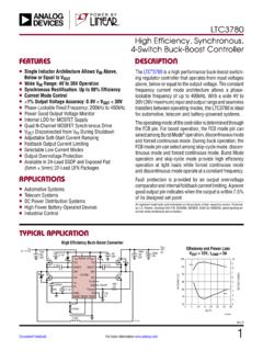
Transcription of LT3080 - Adjustable 1.1A Single Resistor Low Dropout …
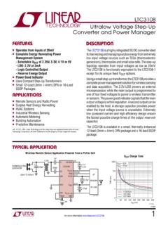
1 Single Resistor Low Dropout RegulatorThe LT 3080 is a low Dropout linear regulator that can be paralleled to increase output current or spread heat in surface mounted boards. Architected as a precision cur-rent source and voltage follower allows this new regulator to be used in many applications requiring high current , adjustability to zero, and no heat sink. Also the device brings out the collector of the pass transistor to allow low Dropout operation down to 350 millivolts when used with multiple key feature of the LT3080 is the capability to supply a wide output voltage range. By using a reference current through a Single Resistor , the output voltage is programmed to any level between zero and 36V. The LT3080 is stable with F of capacitance on the output, and the IC uses small ceramic capacitors that do not require additional ESR as is common with other regulators. Internal protection circuitry includes current limiting and thermal limiting .
2 The LT3080 regulator is offered in the 8-lead MSOP (with an exposed pad for better thermal characteristics), a 3mm 3mm DFN, 5-lead DD-Pak, TO-220 and a simple-to-use 3-lead SOT-223 High current All Surface Mount Supplyn High Efficiency Linear Regulatorn Post Regulator for Switching Suppliesn Low Parts Count Variable Voltage Supplyn Low Output Voltage power Suppliesn Outputs May be Paralleled for Higher current and Heat Spreadingn Output current : Single Resistor Programs Output Voltagen 1% Initial Accuracy of SET Pin Currentn Output Adjustable to 0Vn Low Output Noise: 40 VRMS (10Hz to 100kHz)n Wide Input Voltage Range: to 36Vn Low Dropout Voltage: 350mV (Except SOT-223 Package)n <1mV Load Regulationn < Line Regulationn Minimum Load current : Stable with F Minimum Ceramic Output Capacitorn current Limit with Foldback and Overtemperature Protectedn Available in 8-Lead MSOP, 3mm 3mm DFN, 5-Lead DD-Pak, TO-220 and 3-Lead SOT-223 Variable Output Voltage Supply+ TO 36 VVCONTROLOUT3080 TA01aSET1 FRSETVOUT = RSET 10 AVOUTSet Pin current DistributionSET PIN current distribution ( A) = 13792 Typical applicaTionDescripTionFeaTuresapplicaTio nsL, LT, LTC, LTM, Linear Technology and the Linear logo are registered trademarks and VLDO and ThinSOT are trademarks of Linear Technology Corporation.
3 All other trademarks are the property of their respective owners. LT308023080fcabsoluTe MaxiMuM raTingsVCONTROL Pin Voltage ..40V, Pin Voltage ..40V, Pin current (Note 7) .. 10mASET Pin Voltage (Relative to OUT) .. Short-Circuit Duration ..Indefinite(Note 1)(All Voltages Relative to VOUT)TOP VIEW9 OUTDD PACKAGE8-LEAD (3mm 3mm) PLASTIC DFN56784321 OUTOUTOUTSETININNCVCONTROLTJMAX = 125 C, JA = 64 C/W, JC = 3 C/WEXPOSED PAD (PIN 9) IS OUT, MUST BE SOLDERED TO PCB1234 OUTOUTOUTSET8765 ININNCVCONTROLTOP VIEWMS8E PACKAGE8-LEAD PLASTIC MSOP9 OUT TJMAX = 125 C, JA = 60 C/W, JC = 10 C/WEXPOSED PAD (PIN 9) IS OUT, MUST BE SOLDERED TO PCBQ PACKAGE5-LEAD PLASTIC DD-PAKTAB ISOUTFRONT VIEWINVCONTROLOUTSETNC54321 TJMAX = 125 C, JA = 30 C/W, JC = 3 C/WT PACKAGE5-LEAD PLASTIC TO-220 INVCONTROLOUTSETNCFRONT VIEW54321 TAB ISOUTTJMAX = 125 C, JA = 40 C/W, JC = 3 C/W321 FRONT VIEWTAB ISOUTIN*OUTSETST PACKAGE3-LEAD PLASTIC SOT-223*IN IS VCONTROL AND IN TIED TOGETHERTJMAX = 125 C, JA = 55 C/W, JC = 15 C/WOperating Junction Temperature Range (Notes 2, 10)E-, I-Grades.
4 40 C to 125 CStorage Temperature Range: .. 65 C to 150 CLead Temperature (Soldering, 10 sec) MS8E, Q, T and ST Packages Only ..300 Cpin conFiguraTionLT308033080fcorDer inForMaTionLEAD FREE FINISHTAPE AND REEL PART MARKING*PACKAGE DESCRIPTIONTEMPERATURE RANGELT3080 EDD#PBFLT3080 EDD#TRPBFLCBN8-Lead (3mm x 3mm) Plastic DFN 40 C to 125 CLT3080 IDD#PBFLT3080 IDD#TRPBFLCBN8-Lead (3mm x 3mm) Plastic DFN 40 C to 125 CLT3080 EMS8E#PBFLT3080 EMS8E#TRPBFLTCBM8-Lead Plastic MSOP 40 C to 125 CLT3080 IMS8E#PBFLT3080 IMS8E#TRPBFLTCBM8-Lead Plastic MSOP 40 C to 125 CLT3080EQ#PBFLT3080EQ#TRPBFLT3080Q5-Lead Plastic DD-Pak 40 C to 125 CLT3080IQ#PBFLT3080IQ#TRPBFLT3080Q5-Lead Plastic DD-Pak 40 C to 125 CLT3080ET#PBFLT3080ET#TRPBFLT3080ET5-Lea d Plastic TO-220 40 C to 125 CLT3080IT#PBFLT3080IT#TRPBFLT3080ET5-Lea d Plastic TO-220 40 C to 125 CLT3080 EST#PBFLT3080 EST#TRPBF30803-Lead Plastic SOT-223 40 C to 125 CLT3080 IST#PBFLT3080 IST#TRPBF30803-Lead Plastic SOT-223 40 C to 125 CLEAD BASED FINISHTAPE AND REEL PART MARKING*PACKAGE DESCRIPTIONTEMPERATURE RANGELT3080 EDDLT3080 EDD#TRLCBN8-Lead (3mm x 3mm) Plastic DFN 40 C to 125 CLT3080 IDDLT3080 IDD#TRLCBN8-Lead (3mm x 3mm)
5 Plastic DFN 40 C to 125 CLT3080 EMS8 ELT3080 EMS8E#TRLTCBM8-Lead Plastic MSOP 40 C to 125 CLT3080 IMS8 ELT3080 IMS8E#TRLTCBM8-Lead Plastic MSOP 40 C to 125 CLT3080 EQLT3080EQ#TRLT3080Q5-Lead Plastic DD-Pak 40 C to 125 CLT3080 IQLT3080IQ#TRLT3080Q5-Lead Plastic DD-Pak 40 C to 125 CLT3080 ETLT3080ET#TRLT3080ET5-Lead Plastic TO-220 40 C to 125 CLT3080 ITLT3080IT#TRLT3080ET5-Lead Plastic TO-220 40 C to 125 CLT3080 ESTLT3080 EST#TR30803-Lead Plastic SOT-223 40 C to 125 CLT3080 ISTLT3080 IST#TR30803-Lead Plastic SOT-223 40 C to 125 CConsult LTC Marketing for parts specified with wider operating temperature ranges. *The temperature grade is identified by a label on the shipping more information on lead free part marking, go to: For more information on tape and reel specifications, go to: Pin CurrentISETVIN = 1V, VCONTROL = , ILOAD = 1mA, TJ = 25 C VIN 1V, VCONTROL , 1mA ILOAD (Note 9) A AOutput Offset Voltage (VOUT VSET) VIN = 1V, VCONTROL = 2V, IOUT = 1mAVOSDFN and MSOP Package l 2 mVSOT-223, DD-Pak and T0-220 Package l 5 65 6mV mVLoad Regulation ISET VOS ILOAD = 1mA to ILOAD = 1mA to (Note 8) l mVLine Regulation (Note 9) DFN and MSOP Package ISET VOSVIN = 1V to 25V, VCONTROL = 2V to 25V, ILOAD = 1mA VIN = 1V to 25V, VCONTROL = 2V to 25V, ILOAD = 1mAl mV/VLine Regulation (Note 9) SOT-223, DD-Pak and T0-220 Package ISET VOSVIN = 1V to 26V, VCONTROL = 2V to 26V, ILOAD = 1mA VIN = 1V to 26V, VCONTROL = 2V to 26V, ILOAD = mV/VMinimum Load current (Notes 3, 9)VIN = VCONTROL = 10V VIN = VCONTROL = 25V (DFN and MSOP Package) VIN = VCONTROL = 26V (SOT-223, DD-Pak and T0-220 Package)
6 L l l300500 1 1 A mA mAVCONTROL Dropout Voltage (Note 4)ILOAD = 100mA ILOAD = VVIN Dropout Voltage (Note 4)ILOAD = 100mA ILOAD = l100 350200 500mV mVVCONTROL Pin CurrentILOAD = 100mA ILOAD = l4 176 30mA mACurrent LimitVIN = 5V, VCONTROL = 5V, VSET = 0V, VOUT = 0 . Amplifier RMS Output Noise (Note 6)ILOAD = , 10Hz f 100kHz, COUT = 10 F, CSET = F40 VRMSR eference current RMS Output Noise (Note 6)10Hz f 100kHz1nARMSR ipple Rejectionf = 120Hz, VRIPPLE = , ILOAD = , CSET = F, COUT = F f = 10kHz f = 1 MHz75 55 20dB dB dBThermal Regulation, ISET10ms 1: Stresses beyond those listed under Absolute Maximum Ratings may cause permanent damage to the device. Exposure to any Absolute Maximum Rating condition for extended periods may affect device reliability and 2: Unless otherwise specified, all voltages are with respect to VOUT. The LT3080 is tested and specified under pulse load conditions such that TJ TA.
7 The LT3080E is tested at TA = 25 C. Performance of the LT3080E over the full 40 C and 125 C operating temperature range is assured by design, characterization, and correlation with statistical process controls. The LT3080I is guaranteed over the full 40 C to 125 C operating junction temperature range. Note 3: Minimum load current is equivalent to the quiescent current of the part. Since all quiescent and drive current is delivered to the output of the part, the minimum load current is the minimum current required to maintain regulation. Note 4: For the LT3080 , Dropout is caused by either minimum control voltage (VCONTROL) or minimum input voltage (VIN). Both parameters are specified with respect to the output voltage. The specifications represent the minimum input-to-output differential voltage required to maintain 5: The VCONTROL pin current is the drive current required for the output transistor. This current will track output current with roughly a 1:60 ratio.
8 The minimum value is equal to the quiescent current of the 6: Output noise is lowered by adding a small capacitor across the voltage setting Resistor . Adding this capacitor bypasses the voltage setting Resistor shot noise and reference current noise; output noise is then equal to error amplifier noise (see Applications Information section).Note 7: SET pin is clamped to the output with diodes. These diodes only carry current under transient 8: Load regulation is Kelvin sensed at the 9: current limit may decrease to zero at input-to-output differential voltages (VIN VOUT) greater than 25V (DFN and MSOP package) or 26V (SOT-223, DD-Pak and T0-220 Package). Operation at voltages for both IN and VCONTROL is allowed up to a maximum of 36V as long as the difference between input and output voltage is below the specified differential (VIN VOUT) voltage. Line and load regulation specifications are not applicable when the device is in current 10: This IC includes overtemperature protection that is intended to protect the device during momentary overload conditions.
9 Junction temperature will exceed the maximum operating junction temperature when overtemperature protection is active. Continuous operation above the specified maximum operating junction temperature may impair device 11: The SOT-223 package connects the IN and VCONTROL pins together internally. Therefore, test conditions for this pin follow the VCONTROL conditions listed in the Electrical Characteristics characTerisTics The l denotes the specifications which apply over the full operating temperature range, otherwise specifications are at TA = 25 C. (Note 11)LT308053080fcSet Pin CurrentSet Pin current DistributionOffset Voltage (VOUT VSET)Offset VoltageOffset VoltageLoad RegulationMinimum Load CurrentDropout Voltage (Minimum IN Voltage)TEMPERATURE ( C) 50 SET PIN current ( A) PIN current distribution ( A) = 13792 TEMPERATURE ( C) 50 OFFSET VOLTAGE (mV) G03 = 1mAVOS distribution (mV)23080 G04 101 2N = 13250 INPUT-TO-OUTPUT VOLTAGE (V)0 OFFSET VOLTAGE (mV) G05 *ILOAD = 1mA*SEE NOTE 9 IN ELECTRICALCHARACTERISTICS TABLELOAD current (A)0 OFFSET VOLTAGE (mV) G06 = 25 CTJ = 125 CTEMPERATURE ( C) 50 CHANGE IN OFFSET VOLTAGE WITH LOAD (mV)CHANGE IN REFERENCE current WITH LOAD (nA) G07 2525751250 200 40 6020 30 10 5010 ILOAD = 1mA TO VOUT = 2 VCHANGE IN REFERENCE CURRENTCHANGE IN OFFSET VOLTAGE(VOUT VSET)TEMPERATURE ( C) 50 MINIMUM LOAD current (mA)
10 , CONTROL VOUT = 36V*VIN, CONTROL VOUT = *SEE NOTE 9 IN ELECTRICALCHARACTERISTICS TABLEOUTPUT current (A)0 MINIMUM IN VOLTAGE (VIN VOUT) (mV) = 25 CTJ = 125 COffset Voltage DistributionTypical perForMance characTerisTicsLT308063080fcTypical perForMance characTerisTicsTIME ( s)0 OUTPUT VOLTAGEDEVIATION (mV)LOAD current (mA) 252575403080 G15400200 500503001000105201530 35452550 VOUT = = FVIN = VCONTROL = 3 VCOUT = 10 F CERAMICCOUT = F CERAMICD ropout Voltage (Minimum IN Voltage) Dropout Voltage (Minimum VCONTROL Pin Voltage) Dropout Voltage (Minimum VCONTROL Pin Voltage) current LimitLoad Transient ResponseTEMPERATURE ( C) 50 MINIMUM IN VOLTAGE (VIN VOUT) (mV)2003001503080 G101000050100 25257512540015025050350 ILOAD = = 500mAILOAD = 100mAOUTPUT current (A)0 MINIMUM CONTROL VOLTAGE (VCONTROL VOUT) (V) = 125 CTJ = 50 CTJ = 25 CTEMPERATURE ( C) 50 MINIMUM CONTROL VOLTAGE (VCONTROL VOUT) (V) = = 1mACurrent LimitTEMPERATURE ( C) 50 current LIMIT (A) = 7 VVOUT = 0 VINPUT-TO-OUTPUT DIFFERENTIAL (V)0 current LIMIT (A) *SOT-223, DD-PAKAND TO-220 MSOPANDDFNTJ = 25 C*SEE NOTE 9 IN ELECTRICALCHARACTERISTICS TABLETIME ( s)0 OUTPUT VOLTAGEDEVIATION (mV)LOAD current (A) 5050150403080 35452550 VIN = VCONTROL = 3 VVOUT = = 10 F CERAMICCSET = FLoad Transient ResponseLine Transient ResponseTIME ( s)0IN/CONTROL VOLTAGE (V)OUTPUT VOLTAGEDEVIATION (mV) 252575803080 G1764 500505322010403060 709050100 VOUT = = 10mACOUT = F CERAMICCSET = F CERAMICTurn-On ResponseTIME ( s)0 OUTPUT VOLTAGE (V)INPUT VOLTAGE (V)
