Transcription of LT3481 - 36V, 2A, 2.8MHz Step-Down Switching Regulator ...
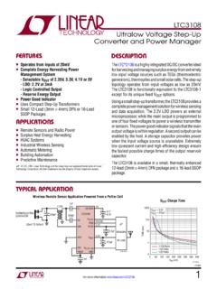
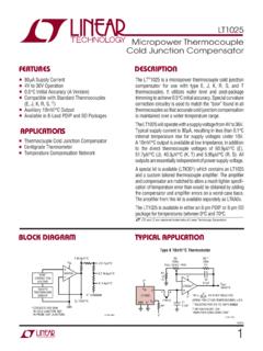
1 LT348113481fc36V, 2A, Step-Down Switching Regulator with 50 A Quiescent CurrentThe LT 3481 is an adjustable frequency (300kHz to ) monolithic buck Switching Regulator that accepts input voltages up to 34V (36V maximum). A high effi ciency switch is included on the die along with a boost Schottky diode and the necessary oscillator, control, and logic circuitry. Current mode topology is used for fast transient response and good loop stability. Low ripple Burst Mode operation maintains high effi ciency at low output currents while keeping output ripple below 15mV in a typical application. In addition, the LT3481 can fur-ther enhance low output current effi ciency by drawing bias current from the output when VOUT is above 3V.
2 Shutdown reduces input supply current to less than 1 A while a resistor and capacitor on the RUN/SS pin provide a controlled output voltage ramp (soft-start). A power good fl ag signals when VOUT reaches 90% of the programmed output voltage. The LT3481 is available in 10-Pin MSOP and 3mm x 3mm DFN packages with exposed pads for low thermal resistance. Automotive Battery Regulation Power for Portable Products Distributed Supply Regulation Industrial Supplies Wall Transformer Regulation Wide Input Range: to 34V Operating, 36V Maximum 2A Maximum Output Current Low Ripple Burst Mode Operation 50 A IQ at 12 VIN to Output Ripple < 15mV Adjustable Switching Frequency: 300kHz to Low Shutdown Current: IQ < 1 A Integrated Boost Diode Power Good Flag Saturating Switch Design: On-Resistance Feedback Reference Voltage Output Voltage.
3 To 20V Soft-Start Capability Synchronizable Between 275kHz to 475kHz Small 10-Pin Thermally Enhanced MSOP and(3mm x 3mm) DFN Step-Down F330pF22 H324kGNDOFF ONLT34813481 TA01 RUN/SSBOOSTEffi ciencyLOAD CURRENT (A) (%)POWER LOSS (mW) = 12 VVOUT = = F = 800 kHz TYPICAL APPLICATION DESCRIPTION FEATURES APPLICATIONSL, LT, LTC, LTM, Burst Mode, Linear Technology and the Linear logo are registered trademarks of Linear Technology Corporation. All other trademarks are the property of their respective , RUN/SS Voltage ..36 VBOOST Pin Voltage ..56 VBOOST Pin Above SW Pin ..30 VFB, RT, VC Voltage ..5V BIAS, PG, BD Voltage ..30 VMaximum Junction 125 C LT3481E, LT3481I.
4 125 CLT3481H .. 150 C(Note 1)Operating Temperature Range (Note 2)LT3481E .. 40 C to 85 40 C to 125 CLT3481H .. 40 C to 150 CStorage Temperature Range .. 65 C to 150 CLead Temperature (Soldering, 10 sec)MSE Only .. 300 C ABSOLUTE MAXIMUM RATINGSTOP VIEWDD PACKAGE10-LEAD (3mm s 3mm) PLASTIC DFNEXPOSED PAD (PIN 11) IS GNDMUST BE CONNECTED TO GND1096784531121 RTVCFBBIASPGBDBOOSTSWVINRUN/SS JA = 43 C/W12345 BDBOOSTSWVINRUN/SS109876 RTVCFBBIASPGTOP VIEWMSE PACKAGE10-LEAD PLASTIC MSOPEXPOSED PAD (PIN 11) IS GNDMUST BE CONNECTED TO GND11 JA = 40 C/W PIN CONFIGURATIONORDER INFORMATIONLEAD FREE FINISHTAPE AND REELPART MARKING*PACKAGE DESCRIPTIONTEMPERATURE RANGELT3481 EDD#PBFLT3481 EDD#TRPBFLBVS10-Lead (3mm 3mm) Plastic DFN 40 C to 85 CLT3481 IDD#PBFLT3481 IDD#TRPBFLBVV10-Lead (3mm 3mm) Plastic DFN 40 C to 125 CLT3481 HDD#PBFLT3481 HDD#TRPBFLBVS10-Lead (3mm 3mm)
5 Plastic DFN 40 C to 150 CLT3481 EMSE#PBFLT3481 EMSE#TRPBFLTBVT10-Lead Plastic MSOP 40 C to 85 CLT3481 IMSE#PBFLT3481 IMSE#TRPBFLTBVW10-Lead Plastic MSOP 40 C to 125 CLT3481 HMSE#PBFLT3481 HMSE#TRPBFLTBVT10-Lead Plastic MSOP 40 C to 150 CLEAD BASED FINISHTAPE AND REELPART MARKING*PACKAGE DESCRIPTIONTEMPERATURE RANGELT3481 EDDLT3481 EDD#TRLBVS10-Lead (3mm 3mm) Plastic DFN 40 C to 85 CLT3481 IDDLT3481 IDD#TRLBVV10-Lead (3mm 3mm) Plastic DFN 40 C to 125 CLT3481 HDDLT3481 HDD#TRLBVS10-Lead (3mm 3mm) Plastic DFN 40 C to 150 CLT3481 EMSELT3481 EMSE#TRLTBVT10-Lead Plastic MSOP 40 C to 85 CLT3481 IMSELT3481 IMSE#TRLTBVW10-Lead Plastic MSOP 40 C to 125 CLT3481 HMSELT3481 HMSE#TRLTBVT10-Lead Plastic MSOP 40 C to 150 CConsult LTC Marketing for parts specifi ed with wider operating temperature ranges.
6 *The temperature grade is identifi ed by a label on the shipping more information on lead free part marking, go to: For more information on tape and reel specifi cations, go to: Input Voltage Current from VINVRUN/SS = AVBIAS = 3V, Not Switching 2260 AVBIAS = 0, Not Switching75120 AQuiescent Current from BIASVRUN/SS = AVBIAS = 3V, Not Switching 50120 AVBIAS = 0, Not Switching05 AMinimum Bias Voltage Pin Bias Current (Note 3)VFB = , VC = 30100nAFB Voltage Line Regulation4V < VIN < Amp gm330 MhoError Amp Gain800VC Source Current65 AVC Sink Current85 AVC Pin to Switch Current Clamp Voltage2 VSwitching FrequencyRT = = = Switch Off-Time 130200nSSwitch Current LimitDuty Cycle = 5% VCESATISW = 2A360mVBoost Schottky Reverse LeakageVSW = 10V, VBIAS = AMinimum Boost Voltage (Note 4)
7 Pin CurrentISW = 1A1835mARUN/SS Pin Current VRUN/SS = ARUN/SS Input Voltage Input Voltage Threshold Offset from Feedback VoltageVFB Rising122mVPG Hysteresis5mVPG LeakageVPG = APG Sink CurrentVPG = 3V 100600 ANote 1: Stresses beyond those listed under Absolute Maximum Ratings may cause permanent damage to the device. Exposure to any Absolute Maximum Rating condition for extended periods may affect device reliability and 2: The LT3481E is guaranteed to meet performance specifi cations from 0 C to 85 C. Specifi cations over the 40 C to 85 C operating temperature range are assured by design, characterization and correlation with statistical process controls. The LT3481I specifi cations are guaranteed over the 40 C to 125 C temperature range.
8 The LT3481H specifi cations are guaranteed over the 40 C to 150 C operating temperature range. High junction temperatures degrade operating lifetimes. Operating lifetime is derated at junction temperatures greater than 125 3: Bias current fl ows into the FB 4: This is the minimum voltage across the boost capacitor needed to guarantee full saturation of the switch. The denotes the specifi cations which apply over the full operating temperature range, otherwise specifi cations are at TA = 25 C. VIN = 10V, VRUNS/SS = 10V VBOOST = 15V, VBIAS = unless otherwise noted.
9 (Note 2)ELECTRICAL CHARACTERISTICSLT348143481fcDUTY CYCLE (%)0 SWITCH CURRENT LIMIT(A)403481 ( C) 50 SUPPLY CURRENT ( A)350253481 G05200100 2505050040030025015075100125 150 VIN = 12 VVOUT = DIODE: DIODES, INC. PDS360 INCREASED SUPPLYCURRENT DUE TO CATCHDIODE LEAKAGE ATHIGH TEMPERATUREEffi ciency (VOUT = )Effi ciency (VOUT = )No Load Supply CurrentNo Load Supply CurrentMaximum Load CurrentLOAD CURRENT (A) (%) G0120106050908070 VIN = 24 VVIN = 12VL: NEC PLC-0745-4R7f: 800kHzLOAD CURRENT (A) (%) G0220106050908070 VIN = 12 VVIN = 24 VVIN = 7VL: NEC PLC-0745-4R7f: 800kHzINPUT VOLTAGE (V)0 SUPPLY CURRENT ( A)70153481 G0440205102010080605030253035TA = 25 CFRONT PAGE APPLICATIONINPUT VOLTAGE (V)5 LOAD CURRENT (A)153481 = = 25 CL = Hf = 800kHzSwitch Current LimitINPUT VOLTAGE (V)5 LOAD CURRENT (A)153481 = = 25 CL = Hf = 800kHzTEMPERATURE ( C) 50 SWITCH CURRENT LIMIT (A) CYCLE = 10 %DUTY CYCLE = 90 %Maximum Load CurrentSwitch Current LimitSWITCHING FREQUENCY (MHz)0 EFFICIENCY (%) = 12 VVIN = 24 VVOUT = = 10 HLOAD = 1 AEffi ciency TYPICAL PERFORMANCE CHARACTERISTICSLT348153481fcBOOST DIODE CURRENT (A)0 BOOST DIODE Vf (V) PIN VOLTAGE (V)0 RUN/SS PIN CURRENT ( A)
10 8101215253481 G176451020303520 Switch Voltage DropBOOST Pin CurrentFeedback VoltageSwitching FrequencyFrequency FoldbackMinimum Switch On-TimeSoft-StartRUN/SS Pin CurrentBoost DiodeSWITCH CURRENT (mA)0400500700150025003481 G10300200500100020003000 35001000600 VOLTAGE DROP (mV)SWITCH CURRENT (mA)00 BOOST PIN CURRENT (mA)103040502000903481 G112010005002500 300015003500607080 TEMPERATURE ( C) 50 FEEDBACK VOLTAGE (V) 1504381 ( C) 50 FREQUENCY (MHz) 1504381 = PIN VOLTAGE (mV)0 Switching FREQUENCY (kHz)8001000120060010003481 G146004002004008001200 14002000RT = ( C) 50 MINIMUM SWITCH ON TIME (ns)80100120253481 G156040 2505075100150125200140 RUN/SS PIN VOLTAGE (V)0 SWITCH CURRENT LIMIT (A) PERFORMANCE CHARACTERISTICSLT348163481fcTEMPERATURE ( C) 50 THRESHOLD VOLTAGE (V) 1503481 25050100 CURRENT LIMIT CLAMPSWITCHING THRESHOLDVC Voltages3481 s/DIVVIN = 12V; FRONT PAGE APPLICATIONILOAD= 10mAFB PIN VOLTAGE (V) 80 VCPIN CURRENT ( A) 60 200201?
