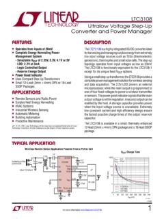
Transcription of LT3999 – Low Noise, 1A, 1MHz Push-Pull DC/DC …
1 LT399913999faFor more information APPLICATION FEATURESDESCRIPTIONLow Noise, 1A, 1 MHz Push-Pull DC/DC Driver with Duty Cycle ControlThe LT 3999 is a monolithic, high voltage, high frequency DC/DC transformer driver providing isolated power in a small solution footprint. The LT3999 has two 1A current limited power switches that switch out of phase. The duty cycle is programmable to adjust the output voltage. The switching frequency is programmed up to 1 MHz and can be synchronized to an external clock for more accurate placement of switcher harmonics. The input operating range is programmed with the precision undervoltage and overvoltage lockouts.
2 The supply current is reduced to less than 1 A during shutdown. A user-defined RC time constant provides an adjustable soft-start capability by limiting the inrush cur-rent at LT3999 is available in a 10-lead MSOP and 3mm 3mm DFN package with exposed pad. 12V to 12V, 10W Low Noise Isolated DC/DC ConverterLT3999 Line Regulation with Duty Cycle ControlAPPLICATIONSn Wide Input Operating Range: to 36Vn Dual 1A Switches with Programmable Current Limit n Programmable Switching Frequency: 50kHz to 1 MHzn Frequency Synchronization Up to 1 MHzn VIN Compensation Using Duty Cycle Control n Low Noise Topology n Programmable Input Over and Undervoltage Lockoutn Cross Conduction Prevention Circuitry n Programmable Soft-Startn Low Shutdown Current.
3 <1 An 10-Lead MSOP and DFN Packagesn Low Noise Isolated Supplies n Medical Instrument and Safetyn Distributed Power n Multiple Output Supplies n Positive-to-Negative Supplies n Noise Immunity in Data Acquisition, RS232 and RS485L, LT, LT C, LT M, Linear Technology and the Linear logo are registered trademarks of Linear Technology Corporation. All other trademarks are the property of their respective owners. VINSYNCUVLOOVLO/DCRDCLT3999 SWA10 F16V255k3999 TA01aRTILIM/SSRBIASINPUT VOLTAGE (V)10 OUTPUT VOLTAGE (V)1214183999 TA01b10812141611131517161113915 IOUT = 200mAIOUT = 800mAIOUT = 400mALT399923999faFor more information CONFIGURATIONABSOLUTE MAXIMUM RATINGSSWA, SWB.
4 To 80 VVIN, UVLO .. to 60 VOVLO/DC, sync .. to 8 VOperating Junction Temper atur e Range (Note 2) LT3999E .. 40 C to 125 C LT3999I .. 40 C to 125 C LT3999H .. 40 C to 150 C LT3999MP .. 55 C to 150 C(Note 1)12345 SWARBIASVINUVLOOVLO/DC109876 SWBILIM/SSSYNCRTRDCTOP VIEW11 GNDMSE PACKAGE10-LEAD PLASTIC MSOP JA = 40 CW, JC = 10 CW EXPOSED PAD (PIN 11) IS GND, MUST BE SOLDERED TO PCBTOP VIEW11 GNDDD PACKAGE10-LEAD (3mm 3mm) PLASTIC DFN10967845321 SWBILIM/SSSYNCRTRDCSWARBIASVINUVLOOVLO/D C JA = 43 C/W, JC = C/W EXPOSED PAD (PIN 11) IS GND, MUST BE SOLDERED TO PCBORDER INFORMATIONLEAD FREE FINISHTAPE AND REELPART MARKING*PACKAGE DESCRIPTIONTEMPERATURE RANGELT3999 EMSE#PBFLT3999 EMSE#TRPBFLTGKR10-Lead Plastic MSOP 40 C to 125 CLT3999 IMSE#PBFLT3999 IMSE#TRPBFLTGKR10-Lead Plastic MSOP 40 C to 125 CLT3999 HMSE#PBFLT3999 HMSE#TRPBFLTGKR10-Lead Plastic MSOP 40 C to 150 CLT3999 MPMSE#PBFLT3999 MPMSE#TRPBFLTGKR10-Lead Plastic MSOP 55 C to 150 CLT3999 EDD#PBFLT3999 EDD#TRPBFLGKQ10-Lead (3mm 3mm) Plastic DFN 40 C to 125 CLT3999 IDD#PBFLT3999 IDD#TRPBFLGKQ10-Lead (3mm 3mm)
5 Plastic DFN 40 C to 125 CConsult LT C Marketing for parts specified with wider operating temperature ranges. *The temperature grade is identified by a label on the shipping LT C Marketing for information on nonstandard lead based finish more information on lead free part marking, go to: For more information on tape and reel specifications, go to: Temper atur e Range .. 65 C to 150 CLead Temper atur e (Soldering, 10 sec) MSOP ..300 CLT399933999faFor more information CHARACTERISTICS The l denotes the specifications which apply over the full operating temperature range, otherwise specifications are at TA = 25 C. VIN = 15 VPARAMETERCONDITIONSMINTYPMAXUNITSI nput Supply and ShutdownVIN Minimum Operating Overvoltage LockoutInternal, Risingl364042 VVIN Supply Current(Note 3) Shutdown CurrentVUVLO = AUVLO Threshold (Rising) Hysteresis125mVUVLO Pin CurrentVUVLO = Threshold (Rising) Hysteresis125mVOVLO/DC Pin CurrentVOVLO/DC = nAPower Switches (SWA, SWB)
6 Switch Saturation Voltage ISW = 1A350mVSwitch Current Limit Internal Overlap Time70nsSwitch Base Drive CurrentISW = 1A35mAOscillator/SyncSwitching FrequencyRT = 316k RT = RT = l 28050 300 1000 320kHz kHz kHzSynchronization Frequency Range1001000kHzSYNC Voltage Pin Input Resistance200k ILIM/SSSWA and SWB Current LimitRILIM/SS = Pin Current10 ADuty CycleSwitch Duty Cycle OVLO/DC = , RDC = , RT = OVLO/DC = , RDC = , RT = OVLO/DC = , RDC = , RT = l 2220 25 48 30% % %Note 1: Stresses beyond those listed under Absolute Maximum Ratings may cause permanent damage to the device. Exposure to any Absolute Maximum Rating condition for extended periods may affect the device reliability and 2: The LT3999E is guaranteed to meet performance specifications from 0 C to 125 C junction temperature.
7 Specifications over the 40 C to 125 C operating junction temperature range are assured by design, characterization, and correlation with statistical process controls. The LT3999I Is guaranteed over the 40 C to 125 C operating junction temperature range. The LT3999H is guaranteed over the full 40 C to 150 C operating junction temperature range. The LT3999MP is 100% tested and guaranteed over the 55 C to 150 C junction temperature range. High junction temperatures degrade operating lifetimes; operating lifetime is derated for junction temperatures greater than 125 3: Supply current specification does not include switch drive currents. Actual supply currents will be more information PERFORMANCE CHARACTERISTICSS witch VCESATS witch Leakage CurrentSwitch Current LimitUVLO Threshold VoltageOVLO Threshold VoltageVIN Shutdown CurrentSwitching FrequencyVCESAT vs Switch CurrentTEMPERATURE ( C) 50 SHUTDOWN CURRENT ( A) 25050100 125 TEMPERAURE ( C) 50 FREQUENCY (kHz)3003501503999 G02250200050100 252575125400275325225375 SWITCH CURRENT (mA)0 SWITCH VCESAT (mV)2002503009008003999 G031501000200400600100100030050070050400 350 TEMPERATURE ( C) 50 SWITCH VCESAT (mV)40050060025751503999 G04300200100 25050100 125 SWITCH CURRENT = 1 ATEMPERATURE ( C) 500 SWITCH CURRENT ( A)
8 252575125 TEMPERATURE ( C) 500 CURRENT LIMIT (mA)200600800100020001400050753999 G06400160018001200 2525100125150 RILIM/SS = OPENRILIM/SS = = ( C) PIN VOLTAGE (V) 2525100125150 UVLO RISINGUVLO FALLINGTEMPERATURE ( C) PIN VOLTAGE (V) 2525100125150 OVLO RISINGOVLO FALLINGLT399953999faFor more information PERFORMANCE CHARACTERISTICSSoft-Start (ILIM/SS) CurrentSwitch Duty CyclePIN FUNCTIONSSWA, SWB (Pin 1, Pin 10): SWA and SWB pins are the open-collector nodes of the power switches. These pins drive the transformer and are connected to the outer ter-minals of the center tapped transformer. Large currents flow through these pins so keep PCB traces short and wide.
9 RBIAS (Pin 2): The RBIAS pin sets the bias current of the power switches (SWA and SWB). Connect the pin to a resistor to (Pin 3): The VIN pin is the main supply pin for the switch driver and internal regulator. Short duration, high current pulses are produced during the turn on and turn off of the power switches. Connect a low ESR capacitor of F or greater. UVLO (Pin 4): The UVLO pin has a precision threshold with hysteresis to implement an accurate VIN undervolt-age lockout. The UVLO function disables switching and sets the part into a low current shutdown mode. Connect the UVLO pin directly to VIN or to a resistor divider (Pin 5): The OVLO/DC pin has a precision thresh-old with hysteresis to implement an accurate VIN overvolt-age lockout.
10 The OVLO function disables the switching. Connect OVLO/DC pin to ground to disable the function or to a resistor divider string to program the duty cycle. RDC (Pin 6): The RDC pin is the duty cycle control pin. A resistor to ground sets the duty cycle. If unused leave the pin floating or connect to the OVLO/DC (Pin 7): The RT pin sets the switching frequency of the power switches. sync (Pin 8): The sync pin synchronizes the part to an external clock. Set the internal oscillator frequency below the external clock frequency. Synchronizing the clock to an external reference is useful for creating more stable positioning of the switcher voltage or current harmonics.
