Transcription of LT6105 - Precision, Rail-to-Rail Input Current Sense …
1 LT6105 . Precision, Extended Input Range Current Sense Amplifier FEATURES DESCRIPTION. n Very Wide, Over-the-Top , Input Common Mode Range The LT 6105 is a micropower, precision Current Sense - Extends 44V Above V (Independent of V +) ampli er with a very wide Input common mode range. - Extends Below V The LT6105 monitors unidirectional Current via the volt- n Wide Power Supply Range: to 36V age across an external Sense resistor. The Input common n Input Offset Voltage: 300 V Maximum mode range extends from to 44V, with respect to n Gain Accuracy: 1% Max the negative supply voltage (V ). This allows the LT6105 . n Gain Con gurable with External Resistors to operate as a high side Current Sense monitor or a low n Operating Current : 150 A side Current Sense monitor. It also allows the LT6105 to n Slew Rate: 2V/ s monitor Current on a negative supply voltage, as well as n Sense Input Current When Powered Down: 1nA continuously monitor a battery from full charge to depletion. n Full-Scale Output Current : 1mA Minimum The inputs of LT6105 can withstand differential voltages n Operating Temperature Range 40 C to 125 C up to 44V, which makes it ideal for monitoring a fuse or n Available in 2mm 3mm DFN and 8-Lead MSOP MOSFET switch.
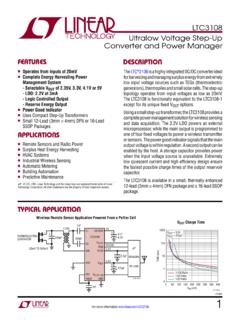
2 Packages Gain is con gured with external resistors from 1V/V to 100V/V. The Input common mode rejection and power APPLICATIONS supply rejection are in excess of 100dB and the Input offset voltage is less than 300 V. A typical slew rate of 2V/ s n High Side or Low Side Current Sensing ensures fast response to unexpected Current changes. n Current Monitoring on Positive or Negative Supply Voltages The LT6105 can operate from an independent power n Battery Monitoring supply of to 36V and draws only 150 A. When n Fuse/MOSFET Monitoring V+ is powered down, the Sense pins are biased off. This n Automotive prevents loading of the monitored circuit, irrespective of n Power Management the Sense voltage. The LT6105 is available in a 6-lead DFN. n Portable Test/Measurement Systems and 8-lead MSOP package. , LT, LTC, LTM and Over-the-Top are registered trademarks of Linear Technology Corporation. All other trademarks are the property of their respective owners. TYPICAL APPLICATION Gain Error vs Input Voltage 4.
3 Gain of 50 Current Sense Ampli er V+ = 12V. 3 VSENSE = 50mV. RIN = 100 . SOURCE. LT6105 A V = 50V. TO 44V 2. RIN2. GAIN ERROR (%). TA = 40 C. VS+ 100 +IN 1. + TA = 25 C. VOUT 0. RIN1 VOUT = 1V/A. 100 IN 1. ROUT TA = 125 C TA = 85 C. VS 2. V+ V . 3. TO LOAD TO 36V 6105 TA01. 4. ( ). VOUT = VS + VS . ROUT. RIN. R. ; A V = OUT ; RIN1 = RIN 2 = RIN. RIN. 0 5 10 15 20 25 30 35. VS+ Input VOLTAGE (V). 40 45. 6105 TA01b 6105fa 1. LT6105 . ABSOLUTE MAXIMUM RATINGS. (Notes 1, 2). Differential Input Voltage (+IN IN) .. 44V Speci ed Temperature Range (Note 5). Input Voltage V(+IN, IN) to V .. to 44V 0 C to 70 C. Total V+ Supply Voltage from V ..36V LT6105I .. 40 C to 85 C. Output Voltage ..V to (V + 36V) LT6105H .. 40 C to 125 C. Output Short-Circuit Duration (Note 3) .. Inde nite Maximum Junction 150 C. Operating Temperature Range (Note 4) Storage Temperature 65 C to 150 C. 40 C to 85 C Lead Temperature (Soldering, 10 sec). LT6105I .. 40 C to 85 C MSOP .. 300 C. LT6105H .. 40 C to 125 C.
4 PIN CONFIGURATION. TOP VIEW. TOP VIEW. IN 1 6 +IN. IN 1 8 +IN. V+ 2 7 5 NC V+ 2 7 NC. NC 3 6 NC. V 3 4 VOUT V 4 5 VOUT. MS8 PACKAGE. DCB PACKAGE 8-LEAD PLASTIC MSOP. 6-LEAD (2mm s 3mm) PLASTIC DFN TJMAX = 150 C, JA = 250 C/W. TJMAX = 150 C, JA = 64 C/W. EXPOSED PAD (PIN 7) CONNECTED TO V (PIN 3). ORDER INFORMATION. LEAD FREE FINISH TAPE AND REEL PART MARKING* PACKAGE DESCRIPTION SPECIFIED TEMPERATURE RANGE. LT6105 CDCB#TRMPBF LT6105 CDCB#TRPBF LCTF 6-Lead (2mm 3mm) Plastic DFN 0 C to 70 C. LT6105 IDCB#TRMPBF LT6105 IDCB#TRPBF LCTF 6-Lead (2mm 3mm) Plastic DFN 40 C to 85 C. LT6105 HDCB#TRMPBF LT6105 HDCB#TRPBF LCTF 6-Lead (2mm 3mm) Plastic DFN 40 C to 125 C. LT6105 CMS8#PBF LT6105 CMS8#TRPBF LTCTD 8-Lead Plastic MS8 0 C to 70 C. LT6105 IMS8#PBF LT6105 IMS8#TRPBF LTCTD 8-Lead Plastic MS8 40 C to 85 C. LT6105 HMS8#PBF LT6105 HMS8#TRPBF LTCTD 8-Lead Plastic MS8 40 C to 125 C. TRM = 500 pieces. *Temperature grades are identi ed by a label on the shipping container. Consult LTC Marketing for parts speci ed with wider operating temperature ranges.
5 Consult LTC Marketing for parts speci ed with wider operating temperature ranges. For more information on lead free part marking, go to: For more information on tape and reel speci cations, go to: 6105fa 2. LT6105 . ELECTRICAL CHARACTERISTICS The l denotes the speci cations which apply over the temperature range 0 C < TA < 70 C (LT6105C), otherwise speci cations are at TA = 25 C. V+ = 12V, V = 0V, VS+ = 12V (see Figure 1), RIN1 = RIN2 = 100 , ROUT = 5k (A V = 50), VSENSE = VS+ VS , unless otherwise speci ed. (Note 5). SYMBOL PARAMETER CONDITIONS MIN TYP MAX UNITS. VS+, VS Input Voltage Range Guaranteed by CMRR 44 V. l 44 V. A V Error Voltage Gain Error (Note 6) VSENSE = 25mV to 75mV, VS+ = 12V 1 1 %. l %. VSENSE = 25mV to 75mV, VS+ = 0V l %. VOS Input Offset Voltage VSENSE = 5mV mV. MS8 Package l mV. Input Offset Voltage VSENSE = 5mV mV. DCB Package l mV. Input Offset Voltage VSENSE = 5mV, VS+ = 0V 1 1 mV. l mV. VOS / T Temperature Coef cient of VOS l V/ C. CMRR Input Common Mode VSENSE = 5mV, VS + = to 44V 100 120 dB.
6 Rejection Ratio l 95 dB. VSENSE = 5mV, VS+ = to 44V 94 dB. VSENSE = 5mV, VS+ = to 44V l 90 dB. V+ Power Supply Voltage Range Guaranteed by PSRR l 36 V. PSRR Power Supply Rejection Ratio VSENSE = 5mV, VS + = 12V, V + = to 36V 98 120 dB. l 94 dB. VSENSE = 5mV, VS+ = 0V, V + = to 36V 98 120 dB. l 94 dB. I(+IN), I( IN) Input Current VSENSE = 0V, VS+ = 3V l 15 25 A. VSENSE = 0V, VS+ = 0V l A. I(+IN) I( IN) Input Offset Current VSENSE = 0V, VS+ = 3V l A. VSENSE = 0V, VS+ = 0V l A. I(+IN) + I( IN) Input Current (Power-Down) V + = 0V, VS+ = 44V, VSENSE = 0V l 1 A. IS V + Supply Current VSENSE = 0V, VS+ = 3V, V+ = l 200 300 A. VSENSE = 0V, VS+ = 3V, V+ = 36V l 240 350 A. VO(MIN) Minimum Output Voltage VSENSE = 0mV, VS+ = 44V, V+ = 36V l 35 mV. VO(MAX) Output High (Referred to V+) VSENSE = 120mV, A V = 100, ROUT = 10k l V. IOUT Maximum Output Current Guaranteed by VO(MAX) l 1 mA. ISC Short-Circuit Output Current VS+ = 44V, VS = 0V, ROUT = 0 l mA. BW 3dB Bandwidth VSENSE = 50mV, A V = 10V/V 100 kHz tS Output Settling to 1% of Final Value VSENSE = 5mV to 100mV 5 s tr Input Step Response (Note 7) VSENSE = 5mV to 100mV 3 s SR Slew Rate (Note 8) VSENSE = 5mV to 150mV, A V = 50V/V, RIN = 400 2 V/ s VREV Reverse Input Voltage I(+IN) + I( IN) = 5mA l 12 V.
7 (Referred to V ). 6105fa 3. LT6105 . ELECTRICAL CHARACTERISTICS The l denotes the speci cations which apply over the temperature range 40 C < TA < 85 C (LT6105I), otherwise speci cations are at TA = 25 C. V+ = 12V, V = 0V, VS+ = 12V (see Figure 1), RIN1 = RIN2 =. 100 , ROUT = 5k (A V = 50), VSENSE = VS+ VS , unless otherwise speci ed. (Note 5). SYMBOL PARAMETER CONDITIONS MIN TYP MAX UNITS. VS+, VS Input Voltage Range Guaranteed by CMRR 44 V. l 44 V. A V Error Voltage Gain Error (Note 6) VSENSE = 25mV to 75mV, VS+ = 12V 1 1 %. l %. VSENSE = 25mV to 75mV, VS+ = 0V l 3 3 %. VOS Input Offset Voltage VSENSE = 5mV mV. MS8 Package l mV. Input Offset Voltage VSENSE = 5mV mV. DCB Package l mV. Input Offset Voltage VSENSE = 5mV, VS+ = 0V 1 1 mV. l mV. VOS / T Temperature Coef cient of VOS l V/ C. CMRR Input Common Mode VSENSE = 5mV, VS+ = to 44V 100 120 dB. Rejection Ratio l 95 dB. VSENSE = 5mV, VS+ = to 44V 94 dB. VSENSE = 5mV, VS+ = to 44V l 90 dB. V+ Power Supply Voltage Range Guaranteed by PSRR l 36 V.
8 PSRR Power Supply Rejection Ratio VSENSE = 5mV, VS+ = 12V, V + = to 36V 98 120 dB. l 94 dB. VSENSE = 5mV, VS+ = 0V, V + = to 36V 98 120 dB. l 94 dB. I(+IN), I( IN) Input Current VSENSE = 0V, VS+ = 3V l 16 27 A. VSENSE = 0V, VS+ = 0V l A. I(+IN) I( IN) Input Offset Current VSENSE = 0V, VS+ = 3V l A. VSENSE = 0V, VS+ = 0V l A. I(+IN) + I( IN) Input Current (Power-Down) V + = 0V, VS+ = 44V, VSENSE = 0V l 1 A. IS V + Supply Current VSENSE = 0V, VS+ = 3V, V+ = l 200 325 A. VSENSE = 0V, VS+ = 3V, V+ = 36V l 250 375 A. VO(MIN) Minimum Output Voltage VSENSE = 0mV, VS+ = 44V, V+ = 36V l 40 mV. VO(MAX) Output High (Referred to V+) VSENSE = 120mV, A V = 100, ROUT = 10k l V. IOUT Maximum Output Current Guaranteed by VO(MAX) l 1 mA. ISC Short-Circuit Output Current VS+ = 44V, VS = 0V, ROUT = 0 l mA. BW 3dB Bandwidth VSENSE = 50mV, A V = 10V/V 100 kHz tS Output Settling to 1% of Final Value VSENSE = 5mV to 100mV 5 s tr Input Step Response (Note 7) VSENSE = 5mV to 100mV 3 s SR Slew Rate (Note 8) VSENSE = 5mV to 150mV, A V = 50V/V, RIN = 400 2 V/ s VREV Reverse Input Voltage I(+IN) + I( IN) = 5mA l 12 V.
9 (Referred to V ). 6105fa 4. LT6105 . ELECTRICAL CHARACTERISTICS The l denotes the speci cations which apply over the temperature range 40 C < TA < 125 C (LT6105H), otherwise speci cations are at TA = 25 C. V+ = 12V, V = 0V, VS+ = 12V (see Figure 1), RIN1 = RIN2 =. 100 , ROUT = 5k (A V = 50), VSENSE = VS+ VS , unless otherwise speci ed. (Note 5). SYMBOL PARAMETER CONDITIONS MIN TYP MAX UNITS. VS+, VS Input Voltage Range Guaranteed by CMRR 44 V. l 44 V. A V Error Voltage Gain Error (Note 6) VSENSE = 25mV to 75mV, VS+ = 12V 1 1 %. l %. VSENSE = 25mV to 75mV, VS+ = 0V l %. VOS Input Offset Voltage VSENSE = 5mV mV. MS8 Package l mV. Input Offset Voltage VSENSE = 5mV mV. DCB Package l mV. Input Offset Voltage VSENSE = 5mV, VS+ = 0V 1 1 mV. l mV. VOS / T Temperature Coef cient of VOS l V/ C. CMRR Input Common Mode VSENSE = 5mV, VS + = to 44V 100 120 dB. Rejection Ratio l 95 dB. VSENSE = 5mV, VS+ = to 44V 94 dB. VSENSE = 5mV, VS+ = to 44V l 80 dB. V+ Power Supply Voltage Range Guaranteed by PSRR l 36 V.
10 PSRR Power Supply Rejection Ratio VSENSE = 5mV, VS + = 12V, V + = to 36V 98 120 dB. l 94 dB. VSENSE = 5mV, VS+ = 0V, V + = to 36V 98 120 dB. l 94 dB. I(+IN), I( IN) Input Current VSENSE = 0V, VS+ = 3V l 18 30 A. VSENSE = 0V, VS+ = 0V l A. I(+IN) I( IN) Input Offset Current VSENSE = 0V, VS+ = 3V l A. VSENSE = 0V, VS+ = 0V l A. I(+IN) + I( IN) Input Current (Power-Down) V + = 0V, VS+ = 44V, VSENSE = 0V l A. IS V + Supply Current VSENSE = 0V, VS+ = 3V, V+ = l 240 350 A. VSENSE = 0V, VS+ = 3V, V+ = 36V l 300 450 A. VO(MIN) Minimum Output Voltage VSENSE = 0mV, VS+ = 44V, V+ = 36V l 45 mV. VO(MAX) Output High (Referred to V+) VSENSE = 120mV, A V = 100, ROUT = 10k l V. IOUT Maximum Output Current Guaranteed by VO(MAX) l 1 mA. ISC Short-Circuit Output Current VS+ = 44V, VS = 0V, ROUT = 0 l mA. BW 3dB Bandwidth VSENSE = 50mV, A V = 10V/V 100 kHz tS Output Settling to 1% of Final Value VSENSE = 5mV to 100mV 5 s tr Input Step Response (Note 7) VSENSE = 5mV to 100mV 3 s SR Slew Rate (Note 8) VSENSE = 5mV to 150mV, A V = 50V/V, RIN = 400 2 V/ s VREV Reverse Input Voltage I(+IN) + I( IN) = 5mA l 12 V.
