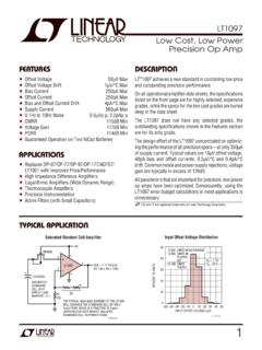
Transcription of LTC1966 - Precision Micropower ΔΣ RMS-to-DC Converter
1 LTC1966 . Precision Micropower RMS-to-DC Converter Features Description n Simple to Use, Requires One Capacitor The LTC 1966 is a true RMS-to-DC Converter that utilizes n True RMS DC Conversion Using Technology an innovative patented computational technique. The n High Accuracy: internal delta sigma circuitry of the LTC1966 makes it sim- Gain Accuracy from 50Hz to 1kHz pler to use, more accurate, lower power and dramatically Total Error from 50Hz to 1kHz more flexible than conventional log antilog RMS-to-DC . n High Linearity: converters. Linearity Allows Simple System Calibration The LTC1966 accepts single-ended or differential input n Low Supply Current: signals (for EMI/RFI rejection) and supports crest factors up 155 A Typ, 170 A Max to 4.
2 Common mode input range is rail-to-rail. Differential n Ultralow Shutdown Current: input range is 1 VPEAK, and offers unprecedented linearity. A Unlike previously available RMS-to-DC converters, the n Constant Bandwidth: superior linearity of the LTC1966 allows hassle free system Independent of Input voltage calibration at any input voltage . 800kHz 3dB, 6kHz 1%. The LTC1966 also has a rail-to-rail output with a separate n Flexible Supplies: output reference pin providing flexible level shifting. The to Single Supply LTC1966 operates on a single power supply from to Up to Dual Supply or dual supplies up to A low power shutdown n Flexible Inputs: mode reduces supply current to A.
3 Differential or Single-Ended Rail-to-Rail Common Mode voltage Range The LTC1966 is insensitive to PC board soldering and Up to 1 VPEAK Differential voltage stresses, as well as operating temperature. The LTC1966 . n Flexible Output: is packaged in the space saving MSOP package which is Rail-to-Rail Output ideal for portable applications. Separate Output reference Pin Allows Level Shifting n Wide Temperature Range: Applications 55 C to 125 C n True RMS Digital Multimeters and Panel Meters n Small Size: n True RMS AC + DC Measurements Space Saving 8-Pin MSOP Package L, LT, LTC, LTM, Linear Technology and the Linear logo are registered trademarks and No Latency DS is a trademark of Linear Technology Corporation.
4 All other trademarks are the property of their respective owners. Protected by Patents including 6359576, 6362677, 6516291 and 6651036. Typical Application Quantum Leap in Linearity Performance LINEARITY ERROR (VOUT mV DC VIN mV ACRMS). LTC1966 , . Single Supply RMS-to-DC Converter 0. TO VDD IN1 OUTPUT. DIFFERENTIAL LTC1966 . CAVE + VOUT. INPUT 1 F CONVENTIONAL. IN2 OUT RTN LOG/ANTILOG. 1966 TA01. F EN VSS GND. OPT. AC. COUPLING 60Hz SINEWAVES. 0 50 100 150 200 250 300 350 400 450 500. VIN (mV ACRMS) 1966 TA01b 1966fb 1. LTC1966 . Absolute Maximum Ratings Pin Configuration (Note 1). Supply voltage VDD to to 7V. VDD to VSS .. to 12V. VSS to 7V to TOP VIEW. Input Currents (Note 2).
5 10mA GND 1 8 ENABLE. Output Current (Note 3).. 10mA IN1 2 7 VDD. IN2 3 6 OUT RTN. ENABLE VSS to VSS + 12V VSS 4 5 VOUT. OUT RTN VSS to VDD MS8 PACKAGE. Operating Temperature Range (Note 4) 8-LEAD PLASTIC MSOP. TJMAX = 150 C, JA = 220 C/W. LTC1966 40 C to 85 C. 40 C to 125 C. 55 C to 125 C. Specified Temperature Range (Note 5). LTC1966 40 C to 85 C. 40 C to 125 C. 55 C to 125 C. Maximum Junction 150 C. Storage Temperature 65 C to 150 C. Lead Temperature (Soldering, 10 sec).. 300 C. Order Information LEAD FREE FINISH TAPE AND REEL PART MARKING* PACKAGE DESCRIPTION TEMPERATURE RANGE. LTC1966 CMS8#PBF LTC1966 CMS8#TRPBF LTTG 8-Lead Plastic MSOP 0 C to 70 C. LTC1966 IMS8#PBF LTC1966 IMS8#TRPBF LTTH 8-Lead Plastic MSOP 40 C to 85 C.
6 LTC1966 HMS8#PBF LTC1966 HMS8#TRPBF LTTG 8-Lead Plastic MSOP 40 C to 125 C. LTC1966 MPMS8#PBF LTC1966 MPMS8#TRPBF LTTG 8-Lead Plastic MSOP 55 C to 125 C. Consult LTC Marketing for parts specified with wider operating temperature ranges. *The temperature grade is identified by a label on the shipping container. For more information on lead free part marking, go to: For more information on tape and reel specifications, go to: Electrical Characteristics The l denotes the specifications which apply over the full operating temperature range, otherwise specifications are at TA = 25 C. VDD = 5V, VSS = 5V, VOUTRTN = 0V, CAVE = 10 F, VIN = 200mVRMS, VENABLE = unless otherwise noted.
7 SYMBOL PARAMETER CONDITIONS MIN TYP MAX UNITS. Conversion Accuracy GERR Conversion Gain Error 50Hz to 1kHz Input (Notes 6, 7) %. LTC1966C, LTC1966I l %. LTC1966H, LTC1966MP l %. VOOS Output Offset voltage (Notes 6, 7) mV. LTC1966C, LTC1966I l mV. LTC1966H, LTC1966MP l mV. LINERR Linearity Error 50mV to 350mV (Notes 7, 8) l %. 1966fb 2. LTC1966 . Electrical Characteristics The l denotes the specifications which apply over the full operating temperature range, otherwise specifications are at TA = 25 C. VDD = 5V, VSS = 5V, VOUTRTN = 0V, CAVE = 10 F, VIN = 200mVRMS, VENABLE = unless otherwise noted. SYMBOL PARAMETER CONDITIONS MIN TYP MAX UNITS. PSRR Power Supply Rejection (Note 9) %V.
8 LTC1966C, LTC1966I l %V. LTC1966H, LTC1966MP l %V. VIOS Input Offset voltage (Notes 6, 7, 10) mV. l mV. Accuracy vs Crest Factor (CF). CF = 4 60Hz Fundamental, 200mVRMS (Note 11) l 1 2 mV. CF = 5 60Hz Fundamental, 200mVRMS (Note 11) l 20 30 mV. Input Characteristics IVR Input voltage Range (Note 14) l VSS VDD V. ZIN Input Impedance Average, Differential (Note 12) 8 M . Average, Common Mode (Note 12) 100 M . CMRRI Input Common Mode Rejection (Note 13) l 7 200 V/V. VIMAX Maximum Input Swing Accuracy = 1% (Note 14) l 1 V. VIMIN Minimum RMS Input l 5 mV. PSRRI Power Supply Rejection VDD Supply (Note 9) l 250 600 V/V. VSS Supply (Note 9) l 120 300 V/V. Output Characteristics OVR Output voltage Range l VSS VDD V.
9 ZOUT Output Impedance VENABLE = (Note 12) l 75 85 95 k . VENABLE = 30 k . CMRRO Output Common Mode Rejection (Note 13) l 16 200 V/V. VOMAX Maximum Differential Output Swing Accuracy = 2%, DC Input (Note 14) V. l V. PSRRO Power Supply Rejection VDD Supply (Note 9) l 250 1000 V/V. VSS Supply (Note 9) l 50 500 V/V. Frequency Response f1P 1% Additional Error (Note 15) CAVE = 10 F 6 kHz f10P 10% Additional Error (Note 15) CAVE = 10 F 20 kHz f 3dB 3dB Frequency (Note 15) 800 kHz Power Supplies VDD Positive Supply voltage l V. VSS Negative Supply voltage (Note 16) l 0 V. IDD Positive Supply Current IN1 = 20mV, IN2 = 0V l 155 170 A. IN1 = 200mV, IN2 = 0V 158 A. ISS Negative Supply Current IN1 = 20mV, IN2 = 0V l 12 20 A.
10 Shutdown Characteristics IDDS Supply Currents VENABLE = l 10 A. ISSS Supply Currents VENABLE = l 1 A. LTC1966H, LTC1966MP l 2 A. IIH ENABLE Pin Current High VENABLE = l A. 1966fb 3. LTC1966 . Electrical Characteristics The l denotes the specifications which apply over the full operating temperature range, otherwise specifications are at TA = 25 C. VDD = 5V, VSS = 5V, VOUTRTN = 0V, CAVE = 10 F, VIN = 200mVRMS, VENABLE = unless otherwise noted. SYMBOL PARAMETER CONDITIONS MIN TYP MAX UNITS. IIL ENABLE Pin Current Low VENABLE = l 2 1 A. LTC1966H, LTC1966MP l 10 A. VTH ENABLE Threshold voltage VDD = 5V, VSS = 5V V. VDD = 5V, VSS = GND V. VDD = , VSS = GND V. VHYS ENABLE Threshold Hysteresis V.