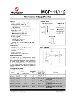
Transcription of LTC2054/LTC2055 - Single/Dual Micropower Zero-Drift ...
1 LTC2054/LTC2055 . Single/Dual Micropower Zero-Drift operational Amplifiers FEATURES DESCRIPTION. n Supply Current 150 A (Max per Ampli er) The LTC 2054/LTC2055 are low power, low noise, single/. Guaranteed from 40 C to 85 C dual, Zero-Drift operational ampli ers with an extended n Offset Voltage 3 V (Max, 40 C to 85 C) temperature version (LTC2054MP) that has guaranteed n Offset Voltage Drift 30nV/ C (Max, 40 C to 85 C) speci cations from 55 C to 150 C. They are available n Guaranteed Speci cations from 55 C to 150 C in TSOT-23 (ThinSOT ) and MS8 packages. For space (LTC2054MP) limited applications, the LTC2055 is also available in a n Common Mode Input Range from V to V + 3mm 3mm dual ne pitch leadless package n Output Swings Rail-to-Rail (DFN).
2 They operate from a single minimum supply n Voltage Gain: 140dB (Typ) and support 5V applications. The current consumption n PSRR and CMRR: 130dB (Typ) is typically 150 A for the LTC2054 and 130 A/amp for n Input Bias Current: 1pA (Typ, 25 C) the LTC2055. n Noise: VP-P ( to 10Hz Typ) The LTC2054/LTC2055 , despite their miniature size, feature n Supply Operation: uncompromising DC performance. The maximum input to 6V ( LTC2054/LTC2055 ) offset voltage and offset drift are V and 30nV/ C over to (LTC2054HV/LTC2055HV) the 40 C to 85 C industrial temperature range. The almost n Low Pro le (1mm) TSOT-23, MS8 and zero DC offset and drift are supported with a power supply 3mm 3mm DFN Packages rejection ratio (PSRR) and common mode rejection ratio APPLICATIONS (CMRR) of 130dB (typ).
3 N Thermocouple Ampli ers The input common mode voltage ranges from the negative n Electronic Scales supply up to typically below the positive supply. The n Medical Instrumentation open-loop gain is typically 140dB. The LTC2054/LTC2055 . n Strain Gauge Ampli ers also feature a VP-P DC to 10Hz noise and a 500kHz n High Resolution Data Acquisition gain-bandwidth product. n DC Accurate RC Active Filters L, LT, LTC, LTM, Linear Technology and the Linear logo are registered trademarks of Linear Technology Corporation. ThinSOT is a trademark of Linear Technology Corporation. All other n Low Side Current Sense trademarks are the property of their respective owners. n Battery-Powered Systems TYPICAL APPLICATION.
4 48V Low Side Precision Current Sense VOS vs Temperature 10. VS = 5V. Q1 10k 8. F 1%. ZETEX 6. ZVN3320F 5V. 4. 100 . 1% 2. VOS ( V). F. 39k LTC2054 VOUT = 100 VSENSE 0. LTC2054. + 2. + F 4. 100 . BZX84C5V1 6. VZ = 8.. 1% 3W. 10. 48V SUPPLY 48V LOAD 55 20 15 50 85 120 155. + 20545 TA01. ISENSE, VSENSE TEMPERATURE ( C). 20545 TA01b 20545fc 1. LTC2054/LTC2055 . ABSOLUTE MAXIMUM RATINGS (Note 1). Total Supply Voltage (V + to V ) Speci ed Temperature Range (Note 2). LTC2054/LTC2055 ..7V LTC2054C/LTC2055C .. 0 C to 70 C. LTC2054 LTC2054 40 C to 85 C. Input Voltage ..(V + + ) to (V S ) LTC2054H/LTC2055H .. 40 C to 125 C. Input 10mA LTC2054MP .. 55 C to 150 C. Output Short-Circuit Duration.
5 Inde nite Storage Temperature 65 C to 150 C. DD Package .. 65 C to 125 C. Lead Temperature (Soldering, 10 sec). TSOT23 and MS8 Packages .. 300 C. PIN CONFIGURATION. TOP VIEW. TOP VIEW OUT A 1 8 V+. TOP VIEW. IN A 2 7 OUT B. OUT 1 5 V+ OUT A 1 8 V+. 2 +IN A 3 6 IN B IN A 2 7 OUT B. V. V 4 5 +IN B +IN A 3 6 IN B. +IN 3 4 IN V 4 5 +IN B. MS8 PACKAGE. S5 PACKAGE DD PACKAGE 8-LEAD PLASTIC MSOP. 5-LEAD PLASTIC TSOT-23 8-LEAD (3mm 3mm) PLASTIC DFN. UNDERSIDE METAL INTERNALLY TJMAX = 150 C, JA = 200 C/W. TJMAX = 150 C, JA = 250 C/W. CONNECTED TO V . (PCB CONNECTION OPTIONAL). TJMAX = 125 C, JA = 160 C/W (NOTE 5). ORDER INFORMATION. LEAD FREE FINISH TAPE AND REEL PART MARKING* PACKAGE DESCRIPTION SPECIFIED TEMPERATURE RANGE.
6 LTC2054CS5#PBF LTC2054CS5#TRPBF LTAGB 5-Lead Plastic TSOT-23 0 C to 70 C. LTC2054 HVCS5#PBF LTC2054 HVCS5#TRPBF LTAGD 5-Lead Plastic TSOT-23 0 C to 70 C. LTC2054IS5#PBF LTC2054IS5#TRPBF LTAGB 5-Lead Plastic TSOT-23 40 C to 85 C. LTC2054 HVIS5#PBF LTC2054 HVIS5#TRPBF LTAGD 5-Lead Plastic TSOT-23 40 C to 85 C. LTC2054HS5#PBF LTC2054HS5#TRPBF LTAGB 5-Lead Plastic TSOT-23 40 C to 125 C. LTC2054 HVHS5#PBF LTC2054 HVHS5#TRPBF LTAGD 5-Lead Plastic TSOT-23 40 C to 125 C. LTC2055 CDD#PBF LTC2055 CDD#TRPBF LBCW 8-Lead (3mm 3mm) Plastic DFN 0 C to 70 C. LTC2055 HVCDD#PBF LTC2055 HVCDD#TRPBF LBCX 8-Lead (3mm 3mm) Plastic DFN 0 C to 70 C. LTC2055 IDD#PBF LTC2055 IDD#TRPBF LBCW 8-Lead (3mm 3mm) Plastic DFN 40 C to 85 C.
7 LTC2055 HVIDD#PBF LTC2055 HVIDD#TRPBF LBCX 8-Lead (3mm 3mm) Plastic DFN 40 C to 85 C. LTC2055 HDD#PBF LTC2055 HDD#TRPBF LBCW 8-Lead (3mm 3mm) Plastic DFN 40 C to 125 C. LTC2055 HVHDD#PBF LTC2055 HVHDD#TRPBF LBCX 8-Lead (3mm 3mm) Plastic DFN 40 C to 125 C. LTC2055 CMS8#PBF LTC2054 CMS8#TRPBF LTBCR 8-Lead Plastic MSOP 0 C to 70 C. LTC2055 HVCMS8#PBF LTC2055 HVCMS8#TRPBF LTBCT 8-Lead Plastic MSOP 0 C to 70 C. LTC2055 IMS8#PBF LTC2055 IMS8#TRPBF LTBCR 8-Lead Plastic MSOP 40 C to 85 C. 20545fc 2. LTC2054/LTC2055 . ORDER INFORMATION. LEAD FREE FINISH TAPE AND REEL PART MARKING* PACKAGE DESCRIPTION SPECIFIED TEMPERATURE RANGE. LTC2055 HVIMS8#PBF LTC2055 HVIMS8#TRPBF LTBCT 8-Lead Plastic MSOP 40 C to 85 C.
8 LTC2055 HMS8#PBF LTC2055 HMS8#TRPBF LTBCR 8-Lead Plastic MSOP 40 C to 125 C. LTC2055 HVHMS8#PBF LTC2055 HVHMS8#TRPBF LTBCT 8-Lead Plastic MSOP 40 C to 125 C. LTC2054 MPS5#PBF LTC2054 MPS5#TRPBF LTFFF 5-Lead Plastic TSOT-23 55 C to 150 C. LTC2054 HVMPS5#PBF LTC2054 HVMPS5#TRPBF LTFFG 5-Lead Plastic TSOT-23 55 C to 150 C. Consult LTC Marketing for parts speci ed with wider operating temperature ranges. *The temperature grade is identi ed by a label on the shipping container. Consult LTC Marketing for information on non-standard lead based nish parts. For more information on lead free part marking, go to: For more information on tape and reel speci cations, go to: ELECTRICAL CHARACTERISTICS ( LTC2054/LTC2055 ) The l denotes the speci cations which apply over the full operating temperature range, otherwise speci cations are at TA = 25 C.
9 VS = 3V, 5V unless otherwise noted. (Note 2). LTC2054C/LTC2055C. LTC2054I/LTC2055I LTC2054H/LTC2055H. SYMBOL PARAMETER CONDITIONS MIN TYP MAX MIN TYP MAX UNITS. IS Supply Current (LTC2054) No Load 140 175 140 180 A. IS Supply Current Per Ampli er No Load 130 150 130 155 A. (LTC2055). VOS Input Offset Voltage (Note 3) 3 3 V. VOS/ T Average Input Offset Drift (Note 3) V/ C. Long-Term Offset Drift 50 50 nV/ mo IB Input Bias Current (Note 4) 1 1 pA. 150 3000 pA. IOS Input Offset Current (Note 4) 2 2 pA. 300 700 pA. en Input Noise Voltage RS = 100 , DC to 1Hz VP-P. RS = 100 , DC to 10Hz VP-P. CMRR Common Mode Rejection Ratio VCM = GND to V + 115 130 115 130 dB. VS = 3V 110 110 dB.
10 VCM = GND to V + 120 130 120 130 dB. VS = 5V 115 115 dB. PSRR Power Supply Rejection Ratio VS = to 6V 120 130 120 130 dB. 115 115 dB. AVOL Large-Signal Voltage Gain RL = 100k, VS = 3V, VOUT = VS /2 120 135 120 135 dB. 115 115 dB. RL = 100k, VS = 5V, VOUT = VS /2 125 140 125 140 dB. 120 120 dB. VOUT Output Voltage Swing High RL = 5k to GND, VS = 3V V. RL = 5k to GND, VS = 3V V. RL = 5k to GND, VS = 5V V. RL = 5k to GND, VS = 5V V. RL = 100k to GND, VS = 3V V. RL = 100k to GND, VS = 3V V. RL = 100k to GND, VS = 5V V. RL = 100k to GND, VS = 5V V. 20545fc 3. LTC2054/LTC2055 . ELECTRICAL CHARACTERISTICS ( LTC2054/LTC2055 ) The l denotes the speci cations which apply over the full operating temperature range, otherwise speci cations are at TA = 25 C.