Transcription of LTC2645 - Quad 12-/10-/8-Bit PWM to VOUT DACs …
1 LTC2645 . Quad 12-/10-/8-Bit PWM. to VOUT DACs with 10ppm/ C Reference Features Description n No Latency PWM-to-Voltage Conversion The LTC 2645 is a family of quad 12-, 10-, and 8-bit PWM- n Voltage Output Updates and Settles within 8 s to-voltage output DACs with an integrated high accuracy, n 100kHz to 30Hz PWM Input Frequency low drift, 10ppm/ C reference in a 16-lead MSOP package. It n Max INL; 1 LSB Max DNL ( LTC2645 -12) has rail-to-rail output buffers and is guaranteed monotonic. n Guaranteed Monotonic n Pin-Selectable Internal or External Reference The LTC2645 measures the period and pulse width of the n to Supply Range PWM input signals and updates the voltage output DACs n to Input Voltage Range after each corresponding PWM input rising edge.
2 The n Low Power: 4mA at 3V, <1 A Power-Down DAC outputs update and settle to 12-bit accuracy within n Guaranteed Operation from 40 C to 125 C. 8 s typically and are capable of sourcing and sinking up n 16-Lead MSOP Package to 5mA (3V) or 10mA (5V), eliminating voltage ripple and replacing slow analog filters and buffer amplifiers. The LTC2645 has a full-scale output of using the Applications 10ppm/ C internal reference. It can operate with an exter- nal reference, which sets the full-scale output equal to the n Digital Calibration external reference voltage. Each DAC enters a pin-selectable n Trimming and Adjustment n idle state when the PWM input is held unchanged for more Level Setting n than 60ms. The part operates from a single to Process Control and Industrial Automation n supply and supports PWM input voltages from to Instrumentation L, LT, LTC, LTM, Linear Technology and the Linear logo are registered trademarks of Linear n Automotive Technology Corporation.
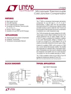
3 All other trademarks are the property of their respective owners. Protected by Patents, including 5396245, 5859606, 6891433, 6937178, 7414561. Typical Application 4-Channel PWM to Voltage Output DAC. PWM Input to DAC Output PWM INPUTS. INA VOUTA. INB VOUTB BUFFERED INA. VOLTAGE 2V/DIV. INC VOUTC OUTPUTS. IND VOUTD. TO LTC2645 . INPUT: 1V TO IOVCC REF. OUTPUT: TO F PD VCC. GND IDLSEL. F F. REFSEL VOUTA. 500mV/DIV. GND. TA01b 2645 TA01a 20 s/DIV. 2645fa For more information 1. LTC2645 . Absolute Maximum Ratings Pin Configuration (Notes 1, 2). Supply Voltages (VCC, IOVCC).. to 6V. INA, INB, INC, to 6V. TOP VIEW. IDLSEL, PD, to 6V VCC 1 16 GND. VOUTA, VOUTB, VOUTC, VOUTA 2. VOUTB 3. 15. 14. VOUTD. VOUTC. to Min (VCC + , 6V) IDLSEL 4.
4 INB 5. 13. 12. REFSEL. REF. to Min (VCC + , 6V) INA 6 11 INC. IOVCC 7 10 IND. Operating Temperature Range GND 8 9 PD. 0 C to 70 C MS PACKAGE. 16-LEAD PLASTIC MSOP. 40 C to 85 C (4mm ). 40 C to 125 C TJMAX = 150 C, JA = 120 C/W. Maximum Junction 150 C. Storage Temperature 65 C to 150 C. Lead Temperature (Soldering, 10 sec).. 300 C. 2645fa 2 For more information LTC2645 . Order Information #orderinfo LTC2645 C MS L 12 #TR PBF. LEAD FREE DESIGNATOR. TAPE AND REEL. TR = 2,500-Piece Tape and Reel RESOLUTION. 12 = 12-Bit 10 = 10-Bit 8 = 8-Bit FULL-SCALE VOLTAGE, INTERNAL REFERENCE MODE. L = PACKAGE TYPE. MS = 16-Lead MSOP. TEMPERATURE GRADE. C = Commercial Temperature Range (0 C to 70 C). I = Industrial Temperature Range ( 40 C to 85 C).
5 H = Automotive Temperature Range ( 40 C to 125 C). PRODUCT PART NUMBER. Consult LTC Marketing for parts specified with wider operating temperature ranges. For more information on lead free part marking, go to: For more information on tape and reel specifications, go to: Some packages are available in 500 unit reels through designated sales channels with #TRMPBF suffix. Product Selection Guide VFS WITH INTERNAL. PART NUMBER PART MARKING* RESOLUTION CHANNELS REFERENCE MAXIMUM INL PACKAGE DESCRIPTION. LTC2645 -L12 645L12 12-Bit 4 16-Lead Plastic MSOP. LTC2645 -L10 645L10 10-Bit 4 16-Lead Plastic MSOP. LTC2645 -L8 2645L8 8-Bit 4 16-Lead Plastic MSOP. *Temperature grades are identified by a label on the shipping container.
6 2645fa For more information 3. LTC2645 . Electrical Characteristics The l denotes the specifications which apply over the full operating temperature range, otherwise specifications are at TA = 25 C. VCC = to , VOUT unloaded unless otherwise specified. LTC2645 -L12/-L10/-L8 (VFS = ). LTC2645 -L8 LTC2645 -L10 LTC2645 -L12. SYMBOL PARAMETER CONDITIONS MIN TYP MAX MIN TYP MAX MIN TYP MAX UNITS. DC Performance Resolution l 8 10 12 Bits Monotonicity VCC = 3V, Internal Ref. (Note 3) l 8 10 12 Bits DNL Differential VCC = 3V, Internal Ref. (Note 3) l 1 LSB. Nonlinearity INL Integral Nonlinearity VCC = 3V, Internal Ref. (Note 3) l 1 1 LSB. ZSE Zero-Scale Error VCC = 3V, Internal Ref., Code = 0 l 5 5 5 mV. VOS Offset Error VCC = 3V, Internal Ref.
7 (Note 4) l 5 5 5 mV. VOSTC VOS Temperature VCC = 3V, Internal Ref. (Note 9) 10 10 10 V/ C. Coefficient GE Gain Error VCC = 3V, Internal Ref. l %FSR. GETC Gain Temperature VCC = 3V, Internal Ref. (Note 9). Coefficient C-grade 10 10 10 ppm/ C. I-grade 10 10 10 ppm/ C. H-grade 10 10 10 ppm/ C. Load Regulation Internal Ref., Mid-Scale, l LSB/mA. VCC = 3V 10%, 5mA IOUT 5mA. VCC = 5V 10%, l LSB/mA. 10mA IOUT 10mA. ROUT DC Output Internal Ref., Mid-Scale, l . Impedance VCC = 3V 10%, 5mA IOUT 5mA. VCC = 5V 10%, l . 10mA IOUT 10mA. SYMBOL PARAMETER CONDITIONS MIN TYP MAX UNITS. VOUT DAC Output Span External Reference 0 to VREF V. Internal Reference 0 to V. PSR Power Supply Rejection VCC = 3V 10% or 5V 10% 80 dB.
8 ISC Short Circuit Output Current (Note 5) VFS = VCC = Sinking Zero-Scale; VOUT Shorted to VCC l 27 48 mA. Sourcing Full-Scale; VOUT Shorted to GND l 28 48 mA. Power Supply VCC Positive Supply Voltage For Specified Performance l V. IOVCC Digital Input Supply Voltage For Specified Performance l ICC Supply Current (Note 6) VCC = 3V, Internal Reference l 4 5 mA. VCC = 5V, Internal Reference l 8 mA. ICC(IOVCC) Supply Current, IOVCC (Note 6) IOVCC = 5V l 25 50 A. ISD Supply Current in Power-Down Mode (Note 6) VCC = 5V, PD = 0V l 5 A. ISD(IOVCC) Supply Current in Power-Down Mode, IOVCC IOVCC = 5V, PD = 0V l 5 A. (Note 6). 2645fa 4 For more information LTC2645 . Electrical Characteristics The l denotes the specifications which apply over the full operating temperature range, otherwise specifications are at TA = 25 C.
9 VCC = to , VOUT unloaded unless otherwise specified. LTC2645 -L12/-L10/-L8 (VFS = ). SYMBOL PARAMETER CONDITIONS MIN TYP MAX UNITS. Reference Input VREF Input Voltage Range l 1 VCC V. Resistance l 120 160 200 k . Capacitance pF. IREF Reference Current, Power-Down Mode DAC Powered Down l A. Reference Output Output Voltage l V. Reference Temperature Coefficient (Note 9) 10 ppm/ C. Output Impedance k . Capacitive Load Driving 10 F. Short Circuit Current VCC = , REF Shorted to GND mA. Digital Inputs (INA, INB, INC, IND, PD). VIH Digital Input High Voltage l IOVCC V. VIL Digital Input Low Voltage l V. ILK Digital Input Leakage INA/INB/INC/IND = GND to IOVCC l 1 A. CIN Digital Input Capacitance (Note 7) l 5 pF.
10 AC Performance ts Settling Time From INA/INB/INC/IND Rising Edge ( 1 LSB at 8 Bits) s (Note 8) ( 1 LSB at 10 Bits) s ( 1 LSB at 12 Bits) s Voltage Output Slew Rate V/ s Capacitive Load Driving 500 pF. Glitch Impulse At Mid-Scale Transition nV s DAC-to-DAC Crosstalk 1 DAC Held at FS, 1 DAC Switched 0 to FS nV s Multiplying Bandwidth External Reference 320 kHz en Output Voltage Noise Density At f = 1kHz, External Reference 180 nV/ Hz At f = 10kHz, External Reference 160 nV/ Hz At f = 1kHz, Internal Reference 200 nV/ Hz At f = 10kHz, Internal Reference 180 nV/ Hz Output Voltage Noise to 10Hz, External Reference 35 nVP-P. to 10Hz, Internal Reference 40 nVP-P. to 200kHz, External Reference 680 nVP-P. to 200kHz, Internal Reference 730 nVP-P.
