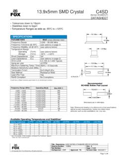
Transcription of LVDS 7 x 5mm 2.5V Oscillator - Oscillators Manufactures
1 Model: FXO-LC72 SERIES Page 1 of 15 FOXE lectronics 5570 Enterprise Parkway Fort Myers, Florida 33905 USA + FAX + EMEA Tel/Fax: +44 . | Asia Hong Kong Tel: + Fax + Taiwan Tel: + Fax + | Japan Tel: + Fax: + 2008 FOX ELECTRONICS | iso9001 :2000 Certified LVDS 7 x 5mm Oscillator Freq: MHz to Applications ANY application requiring an Oscillator SONET Ethernet Storage Area Network Broadband Access Microprocessors / DSP / FPGA Industrial Controllers Test and Measurement Equipment Fiber Channel Contents page Model Selection & Part Number Guide 2 Electrical Characteristic 3 Absolute Maximums 3 Output Wave Characteristics 4 Phase Noise 5 Jitter 5 Pin Assignment 6 Recommended Circuit 6 Reflow
2 6 Mechanical Drawing and Pad Layout 7 Tape and Reel Specification 8 Label 8 Traceability LOT Number & Serial Identification 9 RoHS Material Declaration 10 SGS Report 11 & 12 Mechanical Test 13 Burn-In Test 13 MTTF / FITS calculations 14 Other XPRESSO Links 15 Fox Contact Information 15 Description The Fox XPRESSO Crystal Oscillator is a breakthrough in configurable Frequency Control Solutions.
3 XPRESSO utilizes a family of proprietary ASICs, designed and developed by Fox, with a key focus on noise reduction technologies. The 3rd order Delta Sigma Modulator reduces noise to the levels that are comparable to traditional Bulk Quartz and SAW Oscillators . The ASICs family has ability to select the output type, input voltages, and temperature performance features. With the XPRESS lead-time, low cost, low noise, wide frequency range, excellent ambient performance, XpressO is an excellent choice over the conventional technologies. Finished XPRESSO parts are 100% final tested.
4 OUTPUTE nable / DisableVGNDDDFor more information -- Click on the drawingPRESSXFOXASICsORev. 02/18/2008 Features XTREMELY Low Jitter Low Cost XPRESS Delivery Frequency Resolution to six decimal places Stabilities to 20 PPM -20 to +70 C or -40 to +85 C operating temperatures Tri-State Enable / Disable Feature Industry Standard Package, Footprint & Pin-Out Fully RoHS compliant Gold over Nickel Termination Finish Serial ID with Comprehensive Traceability This part is no longer available from Fox, please contact IDT for this product. FXO-LC72 Series Page 2 of 15 2008 FOX ELECTRONICS | iso9001 :2000 Certified This example, = LVDS Output, Ceramic, 7 x 5mm Package, , 25 PPM Stability, -40 to +85 C Temperature Range, at MHz Model Selection Guide & Fox Part Number 7 7 1B 7 8 1.
5 2 5 1 The 1st Field Product Code # 767A = FXO HC52 768A = FXO HC72 770B = FXO LC52 771B = FXO LC72 773B = FXO PC52 774B = FXO PC72 The 2nd Field The Customer s Frequency The 3rd Field Fox Internally Generated Number (If any specification changes, the last digits change) (The same specs for a different customer also changes the last digits) STEP #2: The Fox Customer Service team provides a customer specific Part Number for use on their Bill Of Materials (BOM). Fox Part Number (The assigned Fox Part Number must be on the BOM not the above Model Description) (This will ensure receipt of the proper part) H = HCMOS L = LVDS P = LVPECL M = LVDS (pin 2 E/D) Q = LVPECL (pin 2 E/D) X = HCMOS (comp 2nd Output) 0 = 100 PPM 5 = 50 PPM 6 = 25 PPM 8 = 20 PPM (-20 ~ +70 C) 5 = 5 x 7 = 7 x 5mm C = Ceramic Q = Quartz blank = -20 C to +70 C R = -40 C to +85 C 3 = V 2 = V F X O L C 7 2 6 R 7 8 1.
6 2 5 Frequency (in MHz) Resolutions to 6 places past the decimal point STEP #1: Customer selects the Model Description and provides to Fox Customer Service Model Description This part is no longer available from Fox, please contact IDT for this Series Page 3 of 15 2008 FOX ELECTRONICS | iso9001 :2000 Certified Electrical Characteristics Parameters Symbol Condition Maximum Value (unless otherwise noted) Frequency Range FO MHz to GHz Frequency Stability 1 100, 50, 25, & 20 ppm Temperature Range TO TSTG Standard operating Optional operating Storage -20 C to +70 C-40 C to +85 C-55 C to +125 C Supply Voltage VDD Standard V 5% Input Current (@ 100 Ohm LOAD)IDD ~ MHz + ~ MHz + ~ MHz + MHz ~ GHz 26 mA 34 mA 44 mA 65 mA Output Load Differential Standard 100 Ohms Typ.
7 Start-Up Time TS10 mSOutput Enable / Disable Time 100 nS Moisture Sensitivity Level MSL JEDEC J-STD-20 1 Termination Finish Au Note 1 Stability is inclusive of 25 C tolerance, operating temperature range, input voltage change, load change, aging, shock and vibration. Absolute Maximum Ratings (Useful life may be impaired. For user guidelines only, not tested) Parameters Symbol Condition Maximum Value (unless otherwise noted) Input Voltage VDD to + Operating Temperature TAMAX 55 C to +105 C Storage Temperature TSTG 55 C to +125 C Junction Temperature 125 CESD Sensitivity HBM Human Body Model >1 kVThis part is no longer available from Fox, please contact IDT for this product.
8 FXO-LC72 Series Page 4 of 15 2008 FOX ELECTRONICS | iso9001 :2000 Certified Note1An optional PIN # 2 as Enable / Disable is available see Model Selection Guide (page 2) Output Wave Characteristics Parameters Symbol Condition Maximum Value (unless otherwise noted) Differential Output Voltage VOD MHz to GHz Typ. Output Offset Voltage VOS Volts DC Typ Output Symmetry (See Drawing Below) @ 50% VP-P Level 45% ~ 55% Output Enable (PIN # 1) Voltage Note1 VIH > 70% VDD Output Disable (PIN # 1) Voltage Note1 VIL < 30% VDD Cycle Rise Time (See Drawing Below) TR 20%~80% 400 pS Cycle Fall Time (See Drawing Below)
9 TF 80%~20% 400 pS Ideally, Symmetry should be 50/50 for 1/2 period -- Other expressions are 45/55 or 55/45 OUTPUT 1 OUTPUT 250% VP-P1/2 PeriodPeriodOscillator SymmetryIdeally, Symmetry should be 50/50 for 1/2 period -- Other expressions are 45/55 or 55/45 Rise Time / Fall Time MeasurementsOUTPUT 1 OUTPUT 250% V P-P OUTPUT 1 20% to 80%OUTPUT 21/2 Period PeriodOscillator SymmetryTR part is no longer available from Fox, please contact IDT for this product. FXO-LC72 Series Page 5 of 15 2008 FOX ELECTRONICS | iso9001 :2000 Certified Jitter is frequency dependent.
10 Below are typical values at select frequencies. Phase Jitter is integrated from HP3048 Phase Noise Measurement System; measured directly into 50 ohm input; VDD = TIE was measured on LeCroy LC684 Digital Storage Scope, directly into 50 ohm input, with Amherst M1 software; VDD = Per MJSQ spec (Methodologies for Jitter and Signal Quality specifications) Rj and Dj, measured on LeCroy LC684 Digital Storage Scope, directly into 50 ohm input, with Amherst M1 software. Per MJSQ spec (Methodologies for Jitter and Signal Quality specifications) LVDS Phase Jitter & Time Interval Error (TIE) Frequency Phase Jitter (12kHz to 20 MHz) T I E (Sigma of Jitter Distribution) Units MHz pS RMS MHz pS RMS MHz pS RMS pS RMS LVDS Random & Deterministic Jitter Composition Frequency Random (Rj) (pS RMS) Deterministic (Dj) (pS P-P) Total Jitter (Tj) (14 x Rj)


![00-10-OE88T-flZ-a 9P1va ) YSn 6LOÊ0 HN 'u.]êles el!ns 9LC ...](/cache/preview/d/4/7/b/d/7/0/e/thumb-d47bd70e2dafb3b15721cd3d5d9684c7.jpg)