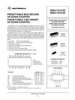
Transcription of March 8 LM78XX/LM78XXA 3-Terminal 1A Positive Voltage ...
1 LM78XX/LM78 XXA 3-Terminal 1A Positive Voltage Regulator March 2008. LM78XX/LM78 XXA. 3-Terminal 1A Positive Voltage Regulator Features General Description Output Current up to 1A The LM78XX series of three terminal Positive regulators Output Voltages of 5, 6, 8, 9, 10, 12, 15, 18, 24 are available in the TO-220 package and with several Thermal Overload Protection fixed output voltages, making them useful in a wide range of applications. Each type employs internal current Short Circuit Protection limiting, thermal shut down and safe operating area pro- Output Transistor Safe Operating Area Protection tection, making it essentially indestructible.
2 If adequate heat sinking is provided, they can deliver over 1A output current. Although designed primarily as fixed Voltage regulators, these devices can be used with external com- ponents to obtain adjustable voltages and currents. Ordering Information Product Number Output Voltage Tolerance Package Operating Temperature LM7805CT 4% TO-220 -40 C to +125 C. LM7806CT. LM7808CT. LM7809CT. LM7810CT. LM7812CT. LM7815CT. LM7818CT. LM7824CT. LM7805 ACT 2% 0 C to +125 C. LM7806 ACT. LM7808 ACT. LM7809 ACT. LM7810 ACT. LM7812 ACT. LM7815 ACT. LM7818 ACT. LM7824 ACT. 2006 Fairchild Semiconductor Corporation 1 LM78XX/LM78 XXA Rev. LM78XX/LM78 XXA 3-Terminal 1A Positive Voltage Regulator Block Diagram Input Series Pass Output Element 1 3.
3 Current SOA. Generator Protection Starting Reference Error Circuit Voltage Amplifier Thermal Protection GND. 2. Figure 1. Pin Assignment TO-220. GND. 1. Input 1 2. GND. 3. Output Figure 2. Absolute Maximum Ratings Absolute maximum ratings are those values beyond which damage to the device may occur. The datasheet specifications should be met, without exception, to ensure that the system design is reliable over its power supply, temperature, and output/input loading variables. Fairchild does not recommend operation outside datasheet specifications. Symbol Parameter Value Unit VI Input Voltage VO = 5V to 18V 35 V. VO = 24V 40 V. R JC Thermal Resistance Junction-Cases (TO-220) 5 C/W.
4 R JA Thermal Resistance Junction-Air (TO-220) 65 C/W. TOPR Operating Temperature LM78xx -40 to +125 C. Range LM78xxA 0 to +125. TSTG Storage Temperature Range -65 to +150 C. 2 LM78XX/LM78 XXA Rev. LM78XX/LM78 XXA 3-Terminal 1A Positive Voltage Regulator Electrical Characteristics (LM7805). Refer to the test circuits. -40 C < TJ < 125 C, IO = 500mA, VI = 10V, CI = F, unless otherwise specified. Symbol Parameter Conditions Min. Typ. Max. Unit VO Output Voltage TJ = +25 C V. 5mA IO 1A, PO 15W, VI = 7V to 20V. Regline Line Regulation(1) TJ = +25 C VO = 7V to 25V 100 mV. VI = 8V to 12V Regload Load Regulation(1) TJ = +25 C IO = 5mA to 100 mV. IO = 250mA to 750mA IQ Quiescent Current TJ = +25 C mA.
5 IQ Quiescent Current Change IO = 5mA to 1A mA. VI = 7V to 25V VO/ T Output Voltage Drift(2) IO = 5mA mV/ C. VN Output Noise Voltage f = 10Hz to 100kHz, TA = +25 C V/VO. RR Ripple Rejection(2) f = 120Hz, VO = 8V to 18V dB. VDROP Dropout Voltage IO = 1A, TJ = +25 C V. rO Output Resistance(2) f = 1kHz m . ISC Short Circuit Current VI = 35V, TA = +25 C 230 mA. (2). IPK Peak Current TJ = +25 C A. notes : 1. Load and line regulation are specified at constant junction temperature. Changes in VO due to heating effects must be taken into account separately. Pulse testing with low duty is used. 2. These parameters, although guaranteed, are not 100% tested in production.
6 3 LM78XX/LM78 XXA Rev. LM78XX/LM78 XXA 3-Terminal 1A Positive Voltage Regulator Electrical Characteristics (LM7806) (Continued). Refer to the test circuits. -40 C < TJ < 125 C, IO = 500mA, VI = 11V, CI = F, CO = F, unless otherwise specified. Symbol Parameter Conditions Min Typ. Max. Unit VO Output Voltage TJ = +25 C V. 5mA IO 1A, PO 15W, VI = to 21V. Regline Line Regulation(3) TJ = +25 C VI = 8V to 25V 120 mV. VI = 9V to 13V (3). Regload Load Regulation TJ = +25 C IO = 5mA to 120 mV. IO = 250mA to 750mA IQ Quiescent Current TJ = +25 C mA. IQ Quiescent Current IO = 5mA to 1A mA. Change VI = 8V to 25V (4). VO/ T Output Voltage Drift IO = 5mA mV/ C.
7 VN Output Noise Voltage f = 10Hz to 100kHz, TA = +25 C V/VO. RR Ripple Rejection(4) f = 120Hz, VO = 8V to 18V dB. VDROP Dropout Voltage IO = 1A, TJ = +25 C V. rO Output Resistance(4) f = 1kHz m . ISC Short Circuit Current VI = 35V, TA = +25 C 250 mA. IPK Peak Current(4) TJ = +25 C A. notes : 3. Load and line regulation are specified at constant junction temperature. Changes in VO due to heating effects must be taken into account separately. Pulse testing with low duty is used. 4. These parameters, although guaranteed, are not 100% tested in production. 4 LM78XX/LM78 XXA Rev. LM78XX/LM78 XXA 3-Terminal 1A Positive Voltage Regulator Electrical Characteristics (LM7808) (Continued).
8 Refer to the test circuits. -40 C < TJ < 125 C, IO = 500mA, VI = 14V, CI = F, CO = F, unless otherwise specified. Symbol Parameter Conditions Min. Typ. Max. Unit VO Output Voltage TJ = +25 C V. 5mA IO 1A, PO 15W, VI = to 23V. Regline Line Regulation(5) TJ = +25 C VI = to 25V 160 mV. VI = to 17V (5). Regload Load Regulation TJ = +25 C IO = 5mA to 160 mV. IO = 250mA to 750mA IQ Quiescent Current TJ = +25 C mA. IQ Quiescent Current Change IO = 5mA to 1A mA. VI = to 25V VO/ T Output Voltage Drift(6) IO = 5mA mV/ C. VN Output Noise Voltage f = 10Hz to 100kHz, TA = +25 C V/VO. RR Ripple Rejection(6) f = 120Hz, VO = to dB. VDROP Dropout Voltage IO = 1A, TJ = +25 C V.
9 RO Output Resistance(6) f = 1kHz m . ISC Short Circuit Current VI = 35V, TA = +25 C 230 mA. IPK Peak Current(6) TJ = +25 C A. notes : 5. Load and line regulation are specified at constant junction temperature. Changes in VO due to heating effects must be taken into account separately. Pulse testing with low duty is used. 6. These parameters, although guaranteed, are not 100% tested in production. 5 LM78XX/LM78 XXA Rev. LM78XX/LM78 XXA 3-Terminal 1A Positive Voltage Regulator Electrical Characteristics (LM7809) (Continued). Refer to the test circuits. -40 C < TJ < 125 C, IO = 500mA, VI = 15V, CI = F, CO = F, unless otherwise specified. Symbol Parameter Conditions Min.
10 Typ. Max. Unit VO Output Voltage TJ = +25 C V. 5mA IO 1A, PO 15W, VI = to 24V. Regline Line Regulation(7) TJ = +25 C VI = to 25V 180 mV. VI = 12V to 17V (7). Regload Load Regulation TJ = +25 C IO = 5mA to 180 mV. IO = 250mA to 750mA IQ Quiescent Current TJ = +25 C mA. IQ Quiescent Current Change IO = 5mA to 1A mA. VI = to 26V VO/ T Output Voltage Drift(8) IO = 5mA mV/ C. VN Output Noise Voltage f = 10Hz to 100kHz, TA = +25 C V/VO. RR Ripple Rejection(8) f = 120Hz, VO = 13V to 23V dB. VDROP Dropout Voltage IO = 1A, TJ = +25 C V. rO Output Resistance(8) f = 1kHz m . ISC Short Circuit Current VI = 35V, TA = +25 C 250 mA. IPK Peak Current(8) TJ = +25 C A.