Transcription of MAX31855 Colnction Compensate ... - Maxim Integrated
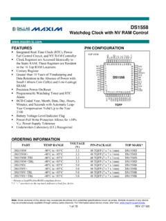
1 General DescriptionThe MAX31855 performs cold-junction compensation and digitizes the signal from a K-, J-, N-, T-, S-, R-, or E-type thermocouple. The data is output in a signed 14-bit, SPI-compatible, read-only format. This converter resolves temperatures to C, allows readings as high as +1800 C and as low as -270 C, and exhibits thermocouple accuracy of 2 C for temperatures ranging from -200 C to +700 C for K-type thermocouples. For full range accuracies and other thermocouple types, see the Thermal Characteristics Industrial Appliances HVACB enefits and Features Integration Reduces Design Time and Lowers System Cost 14-Bit, C Resolution Converter Integrated Cold-Junction Compensation Versions Available for Most Common Thermocouple Types: K-, J-, N-, T-, S-, R-, and E-Type Detects Thermocouple Shorts to GND or VCC Detects Open Thermocouple Interfaces to Most Microcontrollers Simple SPI-Compatible Interface (Read-Only)Ordering Information appears at end of data related parts and recommended products to use with this part, refer to ; Rev 5.
2 1/15 VCCGNDT+ FMAX31855 MAX31855 Cold-Junction CompensatedThermocouple-to-Digital ConverterTypical Application CircuitSupply Voltage Range (VCC to GND).. to + Other to (VCC + )Continuous Power Dissipation (TA = +70 C) SO (derate C above +70 C).. Protection (All Pins, Human Body Model).. 2kVOperating Temperature -40 C to +125 CJunction +150 CStorage Temperature Range .. -65 C to +150 CLead Temperature (soldering, 10s)..+300 CSoldering Temperature (reflow) ..+260 CSO Junction-to-Ambient Thermal Resistance ( JA) ..170 C/W Junction-to-Case Thermal Resistance ( JC) ..40 C/W(Note 1)(TA = -40 C to +125 C, unless otherwise noted.)( VCC P , TA = -40 C to +125 C, unless otherwise noted.)PARAMETERSYMBOLCONDITIONSMINTYPMA XUNITSP ower-Supply VoltageVCC(Note 2) Logic + Logic + CurrentICC9001500 AThermocouple Input Bias CurrentTA = -40 C to +125 C, 100mV across the thermocouple inputs-100+100nAPower-Supply C/VPower-On Reset Voltage ThresholdVPOR(Note 3) Reset Voltage High VoltageVOHIOUT = - Low VoltageVOLIOUT = CompensatedThermocouple-to-Digital Integrated 2 Note 1: Package thermal resistances were obtained using the method described in JEDEC specification JESD51-7, using a four-layer board.
3 For detailed information on package thermal considerations, refer to Maximum RatingsStresses beyond those listed under Absolute Maximum Ratings may cause permanent damage to the device. These are stress ratings only, and functional operation of the device at these or any other conditions beyond those indicated in the operational sections of the specifications is not implied. Exposure to absolute maximum rating conditions for extended periods may affect device Thermal CharacteristicsRecommended Operating ConditionsDC Electrical Characteristics( VCC P , TA = -40 C to +125 C, unless otherwise noted.) (Note 4)PARAMETERSYMBOLCONDITIONSMINTYPMAXUNIT SMAX31855K Thermocouple Temperature Gain and Offset Error ( V/ C nominal sensitivity) (Note 4) TTHERMOCOUPLE = -200 C to +700 C, TA = -20 C to +85 C (Note 3)-2+2 CTTHERMOCOUPLE = +700 C to +1350 C, TA = -20 C to +85 C (Note 3)-4+4 TTHERMOCOUPLE = -270 C to +1372 C, TA = -40 C to +125 C (Note 3)-6+6 MAX31855J Thermocouple Temperature Gain and Offset Error ( V/ C nominal sensitivity) (Note 4)TTHERMOCOUPLE = -210 C to +750 C, TA = -20 C to +85 C (Note 3)-2+2 CTTHERMOCOUPLE = -210 C to +1200 C, TA = -40 C to +125 C (Note 3)-4+4 MAX31855N Thermocouple Temperature Gain and Offset Error ( V/ C nominal sensitivity) (Note 4)TTHERMOCOUPLE = -200 C to +700 C, TA = -20 C to +85 C (Note 3)
4 -2+2 CTTHERMOCOUPLE = +700 C to +1300 C, TA = -20 C to +85 C (Note 3)-4+4 TTHERMOCOUPLE = -270 C to +1300 C, TA = -40 C to +125 C (Note 3)-6+6 MAX31855T Thermocouple Temperature Gain and Offset Error ( V/ C nominal sensitivity) (Note 4)TTHERMOCOUPLE = -270 C to +400 C, TA = -20 C to +85 C (Note 3)-2+2 CTTHERMOCOUPLE = -270 C to +400 C, TA = -40 C to +125 C (Note 3)-4+4 MAX31855E Thermocouple Temperature Gain and Offset Error ( V/ C nominal sensitivity) (Note 4)TTHERMOCOUPLE = -200 C to +700 C, TA = -20 C to +85 C (Note 3)-2+2 CTTHERMOCOUPLE = +700 C to +1000 C, TA = -20 C to +85 C (Note 3)-3+3 TTHERMOCOUPLE = -270 C to +1000 C, TA = -40 C to +125 C (Note 3)-5+5 MAX31855R Thermocouple Temperature Gain and Offset Error ( V/ C nominal sensitivity) (Note 4)TTHERMOCOUPLE = -50 C to +700 C, TA = -20 C to +85 C (Note 3)-2+2 CTTHERMOCOUPLE = +700 C to +1768 C, TA = -20 C to +85 C (Note 3)-4+4 TTHERMOCOUPLE = -50 C to +1768 C, TA = -40 C to +125 C (Note 3)-6+6 MAX31855S Thermocouple Temperature Gain and Offset Error ( V/ C nominal sensitivity) (Note 4)TTHERMOCOUPLE = -50 C to +700 C, TA = -20 C to +85 C (Note 3)-2+2 CTTHERMOCOUPLE = +700 C to +1768 C, TA = -20 C to +85 C (Note 3)-4+4 TTHERMOCOUPLE = -50 C to +1768 C, TA = -40 C to +125 C (Note 3)
5 -6+6 MAX31855 Cold-Junction CompensatedThermocouple-to-Digital Integrated 3 Thermal Characteristics( VCC P , TA = -40 C to +125 C, unless otherwise noted.) (Note 4)(See Figure 1 and Figure 2.)Note 2: All voltages are referenced to GND. Currents entering the IC are specified positive, and currents exiting the IC are 3: Guaranteed by design; not production 4: Not including cold-junction temperature error or thermocouple 5: Specification is 100% tested at TA = +25 C. Specification limits over temperature (TA = TMIN to TMAX) are guaranteed by design and characterization; not production 6: Because the thermocouple temperature conversions begin at VPOR, depending on VCC slew rates, the first thermocouple temperature conversion may not produce an accurate result.
6 Therefore, the tCONV_PU specification is required after VCC is greater than VCCMIN to guarantee a valid thermocouple temperature conversion 7: For all pins except T+ and T- (see the Thermocouple Input Bias Current parameter in the DC Electrical Characteristics table).PARAMETERSYMBOLCONDITIONSMINTYPMA XUNITST hermocouple Temperature Data CInternal Cold-Junction Temperature ErrorTA = -20 C to +85 C (Note 3)-2+2 CTA = -40 C to +125 C (Note 3)-3+3 Cold-Junction Temperature Data ResolutionTA = -40 C to +125 CTemperature Conversion Time (Thermocouple, Cold Junction, Fault Detection)tCONV(Note 5)70100msThermocouple Conversion Power-Up TimetCONV_PU(Note 6)200msPARAMETERSYMBOLCONDITIONSMINTYPMA XUNITSI nput Leakage CurrentILEAK(Note 7)-1+1 AInput CapacitanceCIN8pFSerial-Clock FrequencyfSCL5 MHzSCK Pulse-High WidthtCH100nsSCK Pulse-Low WidthtCL100nsSCK Rise and Fall Time200nsCS Fall to SCK RisetCSS100nsSCK to CS Hold100nsCS Fall to output EnabletDV100nsCS Rise to output DisabletTR40nsSCK Fall to output Data ValidtDO40nsCS Inactive Time(Note 3)200nsMAX31855 Cold-Junction CompensatedThermocouple-to-Digital Integrated 4 Thermal Characteristics (continued)Serial-Interface Timing CharacteristicsFigure 1.
7 Serial-Interface ProtocolFigure 2. Serial-Interface TimingCSSCKSOD31D8D7D6D5D4D3D2D1D0D31D0D 1D2D3 SCKSOtDVtCSStDOCStTRtCHtCLMAX31855 Cold-Junction CompensatedThermocouple-to-Digital Integrated 5 Serial-Interface Diagrams(VCC = + , TA = +25 C, unless otherwise noted.)INTERNAL TEMPERATURE SENSORACCURACYMAX31855 toc02 TEMPERATURE ( C)MEASUREMENT ERROR ( C) = : THIS DATA WAS TAKENIN PRECISION BATH SO HIGHTEMPERATURE LIMIT IS 90 CADC ACCURACY vs. ADC INPUT VOLTAGEACROSS TEMPERATUREMAX31855 toc03 ADC INPUT VOLTAGE (mV)ADC ACCURACY ( C) -40 CVCC = +85 CAT +25 CADC ACCURACY vs. ADC INPUT VOLTAGEACROSS VCCMAX31855 toc04 ADC INPUT VOLTAGE (mV)ADC ACCURACY ( C) = = = TEMPERATURE = +25 CSUPPLY CURRENT vs. TEMPERATUREMAX31855 toc01 TEMPERATURE ( C)SUPPLY CURRENT (mA) = = = Integrated CompensatedThermocouple-to-Digital ConverterTypical Operating CharacteristicsPINNAMEFUNCTION1 GNDG round2T-Thermocouple Input.
8 See Table 1. Do not connect to +Thermocouple Input. See Table Voltage5 SCKS erial-Clock Input6 CSActive-Low Chip Select. Set CS low to enable the serial Output8 DNCDo Not ConnectCSSCKVCC1+287 DNCSOT-T+GNDSOTOP VIEW3465 MAX31855 MAX31855 ADCDIGITALCONTROLCOLD-JUNCTIONCOMPENSATI ONFAULTDETECTIONREFERENCEVOLTAGES4S1S2S3 S5 SCKVCCVCCSOCSGNDT+T- MAX31855 Cold-Junction CompensatedThermocouple-to-Digital Integrated 7 Pin DescriptionPin ConfigurationBlock DiagramDetailed DescriptionThe MAX31855 is a sophisticated thermocouple-to-digital converter with a built-in 14-bit analog-to-digital converter (ADC). The device also contains cold-junction compensa-tion sensing and correction, a digital controller, an SPI-compatible interface, and associated control logic.
9 The device is designed to work in conjunction with an external microcontroller ( C) in thermostatic, process-control, or monitoring applications. The device is available in several versions, each optimized and trimmed for a specific thermo-couple type (K, J, N, T, S, R, or E.). The thermocouple type is indicated in the suffix of the part number ( , MAX31855K). See the Ordering Information table for all ConversionThe device includes signal-conditioning hardware to con-vert the thermocouple s signal into a voltage compatible with the input channels of the ADC. The T+ and T- inputs connect to internal circuitry that reduces the introduction of noise errors from the thermocouple converting the thermoelectric voltages into equiva-lent temperature values, it is necessary to Compensate for the difference between the thermocouple coldjunction side (device ambient temperature) and a 0 C virtual ref-erence.
10 For a K-type thermocouple, the voltage changes by about 41 V/ C, which approximates the thermocouple characteristic with the following linear equation:VOUT = ( V/ C) x (TR - TAMB)where VOUT is the thermocouple output voltage ( V), TR is the temperature of the remote thermocouple junction ( C), and TAMB is the temperature of the device ( C).Other thermocouple types use a similar straight-line approximation but with different gain terms. Note that the MAX31855 assumes a linear relationship between tem-perature and voltage. Because all thermocouples exhibit some level of nonlinearity, apply appropriate correction to the device s output CompensationThe function of the thermocouple is to sense a difference in temperature between two ends of the thermocouple wires.