Transcription of MC14001B Series B-Suffix Series CMOS Gates
1 Semiconductor Components Industries, LLC, 2005 February, 2005 Rev. 41 Publication Order Number: MC14001B /DMC14001B SeriesB- suffix Series cmos GatesMC14001B, MC14011B, MC14023B,MC14025B, MC14071B, MC14073B,MC14081B, MC14082 BThe B Series logic Gates are constructed with P and N channelenhancement mode devices in a single monolithic structure(Complementary MOS). Their primary use is where low powerdissipation and/or high noise immunity is Supply Voltage Range = Vdc to 18 Vdc All Outputs Buffered Capable of Driving Two Low power TTL Loads or One Low powerSchottky TTL Load Over the Rated Temperature Range. Double Diode Protection on All Inputs Except: Triple DiodeProtection on MC14011B and MC14081B Pin for Pin Replacements for Corresponding CD4000 SeriesB suffix Devices Pb Free Packages are Available*MAXIMUM RATINGS (Voltages Referenced to VSS)SymbolParameterValueUnitVDDDC Supply Voltage Range to + , VoutInput or Output Voltage Range(DC or Transient) to VDD + , IoutInput or Output Current(DC or Transient) per Pin 10mAPDP ower Dissipation, per Package(Note 1)500mWTAA mbient Temperature Range 55 to +125 CTstgStorage Temperature Range 65 to +150 CTLLead Temperature(8 Second Soldering)260 CMaximum ratings are those values beyond which device damage can ratings applied to the device are individual stress limit values (notnormal operating conditions) and are not valid simultaneously.
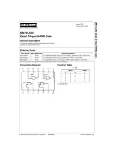
2 If these limits areexceeded, device functional operation is not implied, damage may occur andreliability may be Temperature Derating:Plastic P and D/DW Packages: mW/ C From 65 C To 125 CThis device contains protection circuitry to guard against damage due to highstatic voltages or electric fields. However, precautions must be taken to avoidapplications of any voltage higher than maximum rated voltages to thishigh impedance circuit. For proper operation, Vin and Vout should be constrainedto the range VSS (Vin or Vout) inputs must always be tied to an appropriate logic voltage level( , either VSS or VDD). Unused outputs must be left open.*For additional information on our Pb Free strategy and soldering details, pleasedownload the ON Semiconductor Soldering and Mounting TechniquesReference Manual, INFORMATIONMC14001 BQuad 2 Input NOR GateMC14011 BQuad 2 Input nand GateMC14023 BTriple 3 Input nand GateMC14025 BTriple 3 Input NOR GateMC14071 BQuad 2 Input OR GateMARKINGDIAGRAMS114 PDIP 14P SUFFIXCASE 646MC140xxBCPAWLYYWWSOIC 14D SUFFIXCASE 751 ATSSOP 14DT SUFFIXCASE 948G114140xxBAWLYWW140xxBALYW114xx= Specific Device CodeA= Assembly LocationWL, L= Wafer LotYY, Y= YearWW.
3 W= Work WeekSOEIAJ 14F SUFFIXCASE 965114MC140xxBAWLYWWMC14073 BTriple 3 Input AND GateMC14081 BQuad 2 Input AND GateMC14082 BDual 4 Input AND GateSee detailed ordering and shipping information in the packagedimensions section on page 8 of this data DIAGRAMS12568912133410111256891213341011 125689121334101112568912133410112 INPUT1293 INPUT83465111210131298346511121013129834 651112101311334521011129NC = 6, 8 VDD = PIN 14 VSS = PIN 7 FOR ALL DEVICESNORMC14001 BQuad 2 Input NOR GateMC14025 BTriple 3 Input NOR GateMC14023 BTriple 3 Input nand GateNANDMC14011 BQuad 2 Input nand GateORMC14071 BQuad 2 Input OR GateANDMC14081 BQuad 2 Input AND GateMC14073 BTriple 3 Input AND GateMC14082 BDual 4 Input AND GatePIN ASSIGNMENTS1112131489105432176 OUTCOUTDIN 1 DIN 2 DVDDIN 1 CIN 2 COUTBOUTAIN 2 AIN 1 AVSSIN 2 BIN 1B1112131489105432176 OUTCOUTDIN 1 DIN 2 DVDDIN 1 CIN 2 COUTBOUTAIN 2 AIN 1 AVSSIN 2 BIN 1B1112131489105432176 OUTCIN 1 CIN 2 CIN 3 CVDDIN 3 AOUTAIN 2 BIN 1 BIN 2 AIN 1 AVSSOUTBIN 3B1112131489105432176 OUTCIN 1 CIN 2 CIN 3 CVDDIN 3 AOUTAIN 2 BIN 1 BIN 2 AIN 1 AVSSOUTBIN 3B1112131489105432176 OUTCOUTDIN 1 DIN 2 DVDDIN 1 CIN 2 COUTBOUTAIN 2 AIN 1 AVSSIN 2 BIN 1B1112131489105432176 OUTCIN 1
4 CIN 2 CIN 3 CVDDIN 3 AOUTAIN 2 BIN 1 BIN 2 AIN 1 AVSSOUTBIN 3B1112131489105432176 OUTCOUTDIN 1 DIN 2 DVDDIN 1 CIN 2 COUTBOUTAIN 2 AIN 1 AVSSIN 2 BIN 1B1112131489105432176IN 2 BIN 3 BIN 4 BOUTBVDDNCIN 1 BIN 3 AIN 2 AIN 1 AOUTAVSSNCIN 4 ANC = NO CONNECTIONMC14023 BTriple 3 Input nand GateMC14001 BQuad 2 Input NOR GateMC14011 BQuad 2 Input nand GateMC14082 BDual 4 Input AND GateMC14081 BQuad 2 Input AND GateMC14025 BTriple 3 Input NOR GateMC14071 BQuad 2 Input OR GateMC14073 BTriple 3 Input AND GateMC14001B ELECTRICAL CHARACTERISTICS (Voltages Referenced to VSS) VDD 55 C 25 C 125 C Characteristic Symbol VDDVdc Min Max Min Typ (2) Max Min Max Unit Output Voltage 0 LevelVin = VDD or 0 VOL 000 Vdc 1 LevelVin = 0 or VDD VOH Vdc Input Voltage 0 Level(VO = or Vdc) (VO = or Vdc) (VO = or Vdc)
5 VIL Vdc 1 Level(VO = or Vdc) (VO = or Vdc) (VO = or Vdc) VIH Vdc Output Drive Current(VOH = Vdc) Source(VOH = Vdc)(VOH = Vdc)(VOH = Vdc) IOH mAdc (VOL = Vdc) Sink(VOL = Vdc)(VOL = Vdc) IOL mAdc Input Current Iin 15 Adc Input Capacitance(Vin = 0) Cin pF Quiescent Current(Per Package)
6 IDD Adc Total Supply Current (3) (4)(Dynamic plus Quiescent,Per gate , CL = 50 pF) IT IT = ( A/kHz) f + IDD/NIT = ( A/kHz) f + IDD/NIT = ( A/kHz) f + IDD/N Adc2. Data labelled Typ is not to be used for design purposes but is intended as an indication of the IC s potential The formulas given are for the typical characteristics only at 25 To calculate total supply current at loads other than 50 pF:IT(CL) = IT(50 pF) + (CL 50) Vfkwhere: IT is in A (per package), CL in pF, V = (VDD VSS) in volts, f in kHz is input frequency, and k = x the number of exercised gatesper Series gate SWITCHING TIMES SWITCHING CHARACTERISTICS (5) (CL = 50 pF, TA = 25 C) Characteristic Symbol VDDVdc Min Typ (6) Max Unit Output Rise Time, All B Series GatestTLH = ( ns/pF) CL + 33 nstTLH = ( ns/pF) CL + 20 nstTLH = ( ns/PF)
7 CL + 20 ns tTLH 1005040 20010080 ns Output Fall Time, All B Series GatestTHL = ( ns/pF) CL + 33 nstTHL = ( ns/pF) CL + 20 nstTHL = ( ns/pF) CL + 20 ns tTHL 1005040 20010080 ns Propagation Delay TimeMC14001B, MC14011B onlytPLH, tPHL = ( ns/pF) CL + 80 nstPLH, tPHL = ( ns/pF) CL + 32 nstPLH, tPHL = ( ns/pF) CL + 27 nsAll Other 2, 3, and 4 Input GatestPLH, tPHL = ( ns/pF) CL + 115 nstPLH, tPHL = ( ns/pF) CL + 47 nstPLH, tPHL = ( ns/pF) CL + 37 ns8 Input Gates (MC14068B, MC14078B)tPLH, tPHL = ( ns/pF) CL + 155 nstPLH, tPHL = ( ns/pF) CL + 62 nstPLH, tPHL = ( ns/pF) CL + 47 ns tPLH, tPHL 125504016065502008060 25010080300130100350150110 ns5.
8 The formulas given are for the typical characteristics only at 25 Data labelled Typ is not to be used for design purposes but is intended as an indication of the IC s potential ns20 nstPHLtPLHtTLHtTHLVOLVOH0 VVDDINPUTOUTPUTINVERTING*All unused inputs of AND, nand Gates must be connected to unused inputs of OR, NOR Gates must be connected to *Figure 1. Switching Time Test Circuit and WaveformsMC14001B SCHEMATICNOR, OR GATES14*7 VSS3, 4, 10, 11 VDDVSSVDD*Inverter omitted in MC14001B1, 6, 8, 132, 5, 9, 1214*79, 6, 10 VSSVDD1, 3, 112, 4, 12 VSSVDDVSSVDD8, 5, 13MC14001B, MC14071 BOne of Four Gates ShownMC14025 BOne of Three Gates Shown*Inverter omitted in MC14025 BCIRCUIT SCHEMATICNAND, AND GATES14*73, 4, 10, 11 VSSVDD*Inverter omitted in MC14011B14*79, 6, 10 VSSVDD*Inverter omitted in MC14023B2, 5, 9, 121, 6, 8, 132, 4, 121, 3, 11 VDDVDDVSSVSS8, 5, 13MC14011B, MC14081 BOne of Four Gates ShownMC14023B, MC14073 BOne of Three Gates ShownMC14001B B Series gate CHARACTERISTICSN CHANNEL DRAIN CURRENT (SINK)P CHANNEL DRAIN CURRENT (SOURCE)- 40 C+ 85 C+ 125 CFigure 2.
9 VGS = VdcFigure 3. VGS = , DRAIN-TO-SOURCE VOLTAGE (Vdc)- = - 55 CFigure 4. VGS = 10 VdcFigure 5. VGS = 10 6. VGS = 15 VdcFigure 7. VGS = 15 Vdc0000- 40 C+ 25 C+ 85 C+ 125 C- , DRAIN-TO-SOURCE VOLTAGE (Vdc)TA = - 55 C+ 25 CTA = - 55 C- 40 C+ 25 C+ 85 C+ 125 CVDS, DRAIN-TO-SOURCE VOLTAGE (Vdc)VDS, DRAIN-TO-SOURCE VOLTAGE (Vdc)VDS, DRAIN-TO-SOURCE VOLTAGE (Vdc)VDS, DRAIN-TO-SOURCE VOLTAGE (Vdc)TA = - 55 C- 40 C+ 25 C+ 85 C+ 125 10- 40- 35- 30- 25- 20- 15- 10- 45- = - 55 C- 40 C+ 25 C+ 85 C- 10- 20- 16- 12- 18- 14- 80- 70- 60- 50- 40- 30- 20- 10- 90- = - 55 C- 40 C+ 25 C+ 85 C- 10I ,DDRAIN CURRENT (mA)I ,DDRAIN CURRENT (mA)I ,DDRAIN CURRENT (mA)I ,DDRAIN CURRENT (mA)I ,DDRAIN CURRENT (mA)I ,DDRAIN CURRENT (mA)+ 125 C+ 125 CThese typical curves are not guarantees, but are design.
10 The maximum rating for output current is 10 mA per B Series gate CHARACTERISTICS (cont d)VOLTAGE TRANSFER CHARACTERISTICSF igure 8. VDD = VdcFigure 9. VDD = 10 , INPUT VOLTAGE (Vdc)SINGLE INPUT nand , ANDMULTIPLE INPUT NOR, ORSINGLE INPUT NOR, ORMULTIPLE INPUT nand , ANDSINGLE INPUT nand , ANDMULTIPLE INPUT NOR, ORSINGLE INPUT NOR, ORMULTIPLE INPUT nand , , INPUT VOLTAGE (Vdc)V ,outOUTPUT VOLTAGE (Vdc)V ,outOUTPUT VOLTAGE (Vdc)Figure 10. VDD = 15 Vdc00 SINGLE INPUT nand , ANDMULTIPLE INPUT NOR, ORSINGLE INPUT NOR, ORMULTIPLE INPUT nand , , INPUT VOLTAGE (Vdc)121416V ,outOUTPUT VOLTAGE (Vdc)DC NOISE MARGINThe DC noise margin is defined as the input voltage rangefrom an ideal 1 or 0 input level which does not produceoutput state change(s). The typical and guaranteed limitvalues of