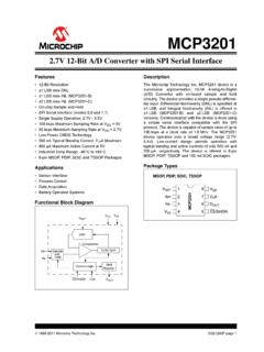
Transcription of MC34063A, MC33063A, SC34063A, SC33063A, 1.5 …
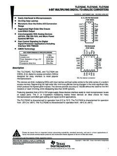
1 mc34063a , mc33063a , sc34063a , sc33063a , NCV33063A. A, Step-Up/Down/. Inverting Switching Regulators The mc34063a Series is a monolithic control circuit containing the MARKING. primary functions required for DC to DC converters. These devices DIAGRAMS. consist of an internal temperature compensated reference, comparator, 8. controlled duty cycle oscillator with an active current limit circuit, 3x063. driver and high current output switch. This series was specifically ALYWA. designed to be incorporated in Step Down and Step Up and G. Voltage Inverting applications with a minimum number of external SOIC 8 1. 8 D SUFFIX. components. Refer to Application Notes AN920A/D and AN954/D. 1 CASE 751 8. for additional design information. 3x063V. Features ALYWA. G. Operation from V to 40 V Input 1. Low Standby Current Current Limiting 8. Output Switch Current to A. 3x063AP1. Output Voltage Adjustable AWL. Frequency Operation to 100 kHz YYWWG.
2 Precision 2% Reference PDIP 8 1. NCV Prefix for Automotive and Other Applications Requiring P, P1 SUFFIX. CASE 626 8. Unique Site and Control Change Requirements; AEC Q100 8. Qualified and PPAP Capable 33063 AVP. 1. AWL. These Devices are Pb Free, Halogen Free/BFR Free and are RoHS YYWWG. Compliant 1. 1. Drive 8 Switch Collector Collector S Q Q2. Q1 DFN8 33063. R ALYWA. Ipk 7 100 CASE 488AF. 2 1 G. Sense Switch Emitter Ipk Oscillator CT. 6 3 x = 3 or 4. VCC Timing Comparator Capacitor A = Assembly Location V L, WL = Wafer Lot +. Reference Y, YY = Year - Regulator W, WW = Work Week Comparator 5 4 G or G = Pb Free Package Inverting GND. Input (Bottom View). This device contains 79 active transistors. Figure 1. Representative Schematic Diagram ORDERING INFORMATION. See detailed ordering and shipping information in the package dimensions section on page 12 of this data sheet. Semiconductor Components Industries, LLC, 2016 1 Publication Order Number: December, 2016 Rev.
3 24 mc34063a /D. mc34063a , mc33063a , sc34063a , sc33063a , NCV33063A. Switch Driver .. 1 8. Collector Collector Switch Collector Driver Collector . Switch 2 7 Ipk Sense Emitter Switch Emitter Ipk Sense . EP Flag Timing 6 Timing Capacitor VCC.. 3 VCC. Capacitor Comparator GND Comparator GND 4 5 Inverting Inverting Input Input (Top View). (Top View). Figure 2. Pin Connections MAXIMUM RATINGS. Rating Symbol Value Unit Power Supply Voltage VCC 40 Vdc Comparator Input Voltage Range VIR to + 40 Vdc Switch Collector Voltage VC(switch) 40 Vdc Switch Emitter Voltage (VPin 1 = 40 V) VE(switch) 40 Vdc Switch Collector to Emitter Voltage VCE(switch) 40 Vdc Driver Collector Voltage VC(driver) 40 Vdc Driver Collector Current (Note 1) IC(driver) 100 mA. Switch Current ISW A. Power Dissipation and Thermal Characteristics Plastic Package, P, P1 Suffix TA = 25 C PD W. Thermal Resistance RqJA 115 C/W. SOIC Package, D Suffix TA = 25 C PD 625 mW.
4 Thermal Resistance RqJA 160 C/W. Thermal Resistance RqJC 45 C/W. DFN Package TA = 25 C PD mW. Thermal Resistance RqJA 80 C/W. Operating Junction Temperature TJ +150 C. Operating Ambient Temperature Range TA C. mc34063a , sc34063a 0 to +70. MC33063AV, NCV33063A 40 to +125. mc33063a , sc33063a 40 to + 85. Storage Temperature Range Tstg 65 to +150 C. Stresses exceeding those listed in the Maximum Ratings table may damage the device. If any of these limits are exceeded, device functionality should not be assumed, damage may occur and reliability may be affected. 1. Maximum package power dissipation limits must be observed. 2. This device series contains ESD protection and exceeds the following tests: Human Body Model 4000 V per MIL STD 883, Method 3015. Machine Model Method 400 V. 3. NCV prefix is for automotive and other applications requiring site and change control. 2. mc34063a , mc33063a , sc34063a , sc33063a , NCV33063A.
5 ELECTRICAL CHARACTERISTICS (VCC = V, TA = Tlow to Thigh [Note 4], unless otherwise specified.). Characteristics Symbol Min Typ Max Unit OSCILLATOR. Frequency (VPin 5 = 0 V, CT = nF, TA = 25 C) fosc 24 33 42 kHz Charge Current (VCC = V to 40 V, TA = 25 C) Ichg 24 35 42 mA. Discharge Current (VCC = V to 40 V, TA = 25 C) Idischg 140 220 260 mA. Discharge to Charge Current Ratio (Pin 7 to VCC, TA = 25 C) Idischg/Ichg . Current Limit Sense Voltage (Ichg = Idischg, TA = 25 C) Vipk(sense) 250 300 350 mV. OUTPUT SWITCH (Note 5). Saturation Voltage, Darlington Connection VCE(sat) V. ( ISW = A, Pins 1, 8 connected). Saturation Voltage (Note 6) VCE(sat) V. (ISW = A, RPin 8 = 82 W to VCC, Forced b ] 20). DC Current Gain (ISW = A, VCE = V, TA = 25 C) hFE 50 75 . Collector Off State Current (VCE = 40 V) IC(off) 100 mA. COMPARATOR. Threshold Voltage Vth V. TA = 25 C TA = Tlow to Thigh Threshold Voltage Line Regulation (VCC = V to 40 V) Regline mV.
6 MC33063, MC34063 MC33063V, NCV33063 Input Bias Current (Vin = 0 V) IIB 20 400 nA. TOTAL DEVICE. Supply Current (VCC = V to 40 V, CT = nF, Pin 7 = VCC, ICC mA. VPin 5 > Vth, Pin 2 = GND, remaining pins open). Product parametric performance is indicated in the Electrical Characteristics for the listed test conditions, unless otherwise noted. Product performance may not be indicated by the Electrical Characteristics if operated under different conditions. 4. Tlow = 0 C for MC34063, SC34063; 40 C for MC33063, SC33063, MC33063V, NCV33063. Thigh = +70 C for MC34063, SC34063; + 85 C for MC33063, SC33063; +125 C for MC33063V, NCV33063. 5. Low duty cycle pulse techniques are used during test to maintain junction temperature as close to ambient temperature as possible. 6. If the output switch is driven into hard saturation (non Darlington configuration) at low switch currents ( 300 mA) and high driver currents ( 30 mA), it may take up to ms for it to come out of saturation.
7 This condition will shorten the off time at frequencies 30 kHz, and is magnified at high temperatures. This condition does not occur with a Darlington configuration, since the output switch cannot saturate. If a non Darlington configuration is used, the following output drive condition is recommended: IC output Forced b of output switch : w 10. IC driver mA *. * The 100 W resistor in the emitter of the driver device requires about mA before the output switch conducts. 3. mc34063a , mc33063a , sc34063a , sc33063a , NCV33063A. 18 180. VCC = V, Pin 7 = VCC. ON TIME (ms), FREQUENCY (kHz). 16 160. Pin 5 = GND, TA = 25 C. V OSC , OSCILLATOR VOLTAGE (V). 14 140. 12 120. OFF TIME (ms). ON TIME (ms). 200 mV/DIV. 10 100. 8 80. 6 60. OFF TIME (ms). 4 40 VCC = V Pins 1, 5, 8 = Open Pin 7 = VCC CT = nF. 2 FREQUENCY (kHz) 20 Pin 2 = GND TA = 25 C. 0 0. 10 ms/DIV. Ct, TIMING CAPACITOR CAPACITANCE (nF) Figure 4. Timing Capacitor Waveform Figure 3.
8 Oscillator Frequency VCE(sat), SATURATION VOLTAGE (V). VCE(sat), SATURATION VOLTAGE (V). Darlington Connection VCC = V. Pin 7 = VCC. Pins 2, 3, 5 = GND Forced b = 20. VCC = V TA = 25 C. Pins 1, 7, 8 = VCC (See Note 7). Pins 3, 5 = GND TA = 25 C. (See Note 7) 0. 0 0 IE, EMITTER CURRENT (A) IC, COLLECTOR CURRENT(A). Figure 5. Emitter Follower Configuration Output Figure 6. Common Emitter Configuration Output Saturation Voltage versus Emitter Current Switch Saturation Voltage versus Collector Current VIPK(sense), CURRENT LIMIT SENSE VOLTAGE (V). 400 380 VCC = V. 360. I CC, SUPPLY CURRENT (mA). Ichg = Idischg 340 320. 300. 280. 260 CT = nF. Pin 7 = VCC. 240. Pin 2 = GND. 220 200 0. -55 -25 0 25 50 75 100 125 0 10 15 20 25 30 35 40. TA, AMBIENT TEMPERATURE ( C) VCC, SUPPLY VOLTAGE (V). Figure 7. Current Limit Sense Voltage Figure 8. Standby Supply Current versus versus Temperature Supply Voltage 7. Low duty cycle pulse techniques are used during test to maintain junction temperature as close to ambient temperature as possible.
9 4. mc34063a , mc33063a , sc34063a , sc33063a , NCV33063A. 170 mH. L. 8 1. 180. S Q Q2. R Q1. 7. 2. 1N5819. Ipk Rsc CT. OSC. 3. Vin 6 VCC CT. 12 V +. 100 V. +. Comp. Ref - Reg 1500. pF. 5 4. mH. R2 Vout 28 V/175 mA Vout 47 k + +. R1 k 330 CO 100. Optional Filter Test Conditions Results Line Regulation Vin = V to 16 V, IO = 175 mA 30 mV = Load Regulation Vin = 12 V, IO = 75 mA to 175 mA 10 mV = Output Ripple Vin = 12 V, IO = 175 mA 400 mVpp Efficiency Vin = 12 V, IO = 175 mA Output Ripple With Optional Filter Vin = 12 V, IO = 175 mA 40 mVpp Figure 9. Step Up Converter 5. mc34063a , mc33063a , sc34063a , sc33063a , NCV33063A. Vout R Vout 8 1 8 1. 7 7. 2 2. Rsc Rsc Vin 6 Vin 6 R 0 for constant Vin Figure 10. External Current Boost Connections for IC Peak Greater than A. 9a. External NPN Switch 9b. External NPN Saturated Switch (See Note 8). 8. If the output switch is driven into hard saturation (non Darlington configuration) at low switch currents ( 300 mA) and high driver currents ( 30 mA), it may take up to ms to come out of saturation.
10 This condition will shorten the off time at frequencies 30 kHz, and is magnified at high temperatures. This condition does not occur with a Darlington configuration, since the output switch cannot saturate. If a non Darlington configuration is used, the following output drive condition is recommended. 6. mc34063a , mc33063a , sc34063a , sc33063a , NCV33063A. 8 1. S Q Q2. R Q1. 7. 2. Rsc Ipk CT. OSC. 1N5819. Vin 6 3. 25 V VCC L 220 mH. + CT. 100 V. + Ref - Comp. 470. Reg pF. 5 4. mH. R2 Vout V/500 mA Vout k + +. R1 k 470 CO 100. Optional Filter Test Conditions Results Line Regulation Vin = 15 V to 25 V, IO = 500 mA 12 mV = Load Regulation Vin = 25 V, IO = 50 mA to 500 mA mV = Output Ripple Vin = 25 V, IO = 500 mA 120 mVpp Short Circuit Current Vin = 25 V, RL = W A. Efficiency Vin = 25 V, IO = 500 mA Output Ripple With Optional Filter Vin = 25 V, IO = 500 mA 40 mVpp Figure 11. Step Down Converter 8 1 1. 8 V. 7 2 7 2.