Transcription of MCP23008/MCP23S08 8-Bit I/O Expander with Serial Interface ...
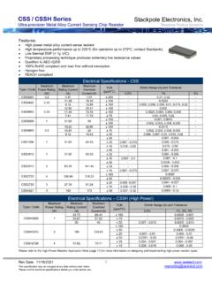
1 2004-2019 Microchip Technology 1 Features 8-Bit Remote Bidirectional I/O Port- I/O pins default to input High-Speed I2C Interface (MCP23008)- 100 kHz- 400 High-Speed SPI Interface (MCP23S08)-10 MHz Hardware Address Pins- Three for the MCP23008 to allow up to eight devices on the bus- Two for the MCP23S08 to allow up to four devices using the same Chip Select Configurable Interrupt Output Pin- Configurable as active-high, active-low or open-drain Configurable Interrupt Source- Interrupt-on-change from configured defaults or pin change Polarity Inversion Register to Configure the Polarity of the Input Port Data External Reset Input Low Standby Current: 1 A (max.) Operating Voltage:- to at -40 C to +85 CI2C at 100 kHzSPI at 5 MHz- to at -40 C to +85 CI2C at 400 kHzSPI at 10 MHz- to at -40 C to +125 CI2C at kHzSPI at 10 MHzPackages 18-pin PDIP (300 mil) 18-pin SOIC (300 mil) 20-pin SSOP 20-pin QFNB lock DiagramGP0GP1GP2GP3GP4GP5GP6GP7 SerialControlGPIOSCLSDARESETINT8 Configuration/8A2:A03 ControlRegistersSerializer/DeserializerI nterruptLogic VDDVSSPORD ecode Interface SCKSISOMCP23S08 MCP23008A1.
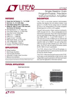
2 A0 MCP23S08 MCP23008/MCP23S088-Bit I/O Expander with Serial Interface 2004-2019 Microchip Technology 2 MCP23008/MCP23S08 Package TypesSDASCLNCINTRESETA1GP4 VDDGP7GP6GP5GP3GP2123456718171615141312 PDIP/SOIC891110GP1GP0A0A2 VSSMCP23008 MCP23008 MCP230081312123456789201918171615141110G P3 VDDGP7GP6GP5GP2GP1GP0N/CGP4 SDASCLVSSA0N/CA1 RESETA2 NCINT SSOPMCP230082019181716678910151413121112 345 QFNSCLSDAVSSA0N/CA1 RESETA2 NCINTGP3 VDDGP7GP6GP5GP2GP1GP0N/CGP4 2004-2019 Microchip Technology 3 MCP23008/MCP23S08 Package Types: (Continued)SISCKCSINTRESETA1GP4 VDDGP7GP6GP5GP3GP2123456718171615141312 PDIP/SOIC891110GP1GP0A0 SOVSSMCP23S08 MCP23S08 MCP23S081312123456789201918171615141110G P3 VDDGP7GP6GP5GP2GP1GP0N/CGP4 SISCKVSSA0N/CA1 RESETSOCSINT SSOPQFNMCP23S082019181716678910151413121 112345 SCKSIVSSA0N/CA1 RESETSOCSINTGP3 VDDGP7GP6GP5GP2GP1GP0N/CGP4 2004-2019 Microchip Technology 4 MCP23008 OVERVIEWThe MCP23X08 device provides 8-Bit , generalpurpose, parallel I/O expansion for I2C bus or SPIapplications.
3 The two devices differ in the number ofhardware address pins and the Serial Interface : MCP23008 I2C Interface ; three address pins MCP23S08 SPI Interface ; two address pinsThe MCP23X08 consists of multiple 8-Bit Configurationregisters for input, output and polarity selection. Thesystem master can enable the I/Os as either inputs oroutputs by writing the I/O Configuration bits. The datafor each input or output is kept in the correspondingInput or Output register. The polarity of the Input Portregister can be inverted with the Polarity Inversionregister. All registers can be read by the system interrupt output can be configured to activateunder two conditions (mutually exclusive) any input state differs from itscorresponding Input Port register state, this isused to indicate to the system master that aninput state has an input state differs from a preconfiguredregister value (DEFVAL register).
4 The Interrupt Capture register captures port values atthe time of the interrupt, thereby saving the conditionthat caused the power -on Reset (POR) sets the registers to theirdefault values and initializes the device state hardware address pins are used to determine thedevice DescriptionsTABLE 1-1:PINOUT DESCRIPTIONPinNamePDIP/SOICQFNSSOPPinTyp eFunctionSCL/SCK1191 ISerial clock data I/O (MCP23008)/ Serial data input (MCP23S08).A2/SO313I/OHardware address input (MCP23008)/ Serial data output (MCP23S08). A2 must be biased address input. Must be biased address input. Must be biased Reset input. Must be biased connect (MCP23008)/External Chip Select input (MCP23S08).INT878 OInterrupt output. Can be configured for active-high, active-low or I/O pin. Can be enabled for interrupt-on-change and/or internal weak pull-up I/O pin. Can be enabled for interrupt-on-change and/or internal weak pull-up I/O pin.
5 Can be enabled for interrupt-on-change and/or internal weak pull-up I/O pin. Can be enabled for interrupt-on-change and/or internal weak pull-up I/O pin. Can be enabled for interrupt-on-change and/or internal weak pull-up I/O pin. Can be enabled for interrupt-on-change and/or internal weak pull-up I/O pin. Can be enabled for interrupt-on-change and/or internal weak pull-up I/O pin. Can be enabled for interrupt-on-change and/or internal weak pull-up 6, 810, 11 2004-2019 Microchip Technology 5 MCP23008 Reset (POR)The on-chip POR circuit holds the device in Reset untilVDD has reached a high enough voltage to deactivatethe POR circuit ( , release the device from Reset).The maximum VDD rise time is specified inSection , Electrical the device exits the POR condition (releasesReset), device operating parameters ( , voltage,temperature, Serial bus frequency, etc.)
6 Must be met toensure proper InterfaceThis block handles the functionality of the I2C(MCP23008) or SPI (MCP23S08) Interface MCP23X08 contains eleven registers that can beaddressed through the Serial Interface block (Table 1-2):TABLE 1-2:REGISTER OPERATION BITThe Sequential Operation (SEQOP) bit (IOCON register) controls the operation of the Address Address Pointer can either be enabled (default) toallow the Address Pointer to increment automaticallyafter each data transfer, or it can be operating in Sequential mode( = 0), the Address Pointer automati-cally increments to the next address after each byteis operating in Byte mode ( = 1),the MCP23X08 does not increment its addresscounter after each byte during the data transfer. Thisgives the ability to continually read the same addressby providing extra clocks (without additional controlbytes).
7 This is useful for polling the GPIO register fordata Write OperationThe I2C Write operation includes the control byte andregister address sequence, as shown in the bottom ofFigure 1-1. This sequence is followed by eight bits ofdata from the master and an Acknowledge (ACK) fromthe MCP23008. The operation is ended with a STOPor RESTART condition being generated by the is written to the MCP23008 after every bytetransfer. If a STOP or RESTART condition isgenerated during a data transfer, the data will not bewritten to the writes and sequential writes are both supportedby the MCP23008. The MCP23008 increments itsaddress counter after each ACK during the Read OperationThe I2C Read operation includes the control bytesequence, as shown in the bottom of Figure 1-1. Thissequence is followed by another control byte (includ-ing the START condition and ACK) with the R/W bitequal to a logic 1 (R/W = 1).
8 The MCP23008 thentransmits the data contained in the addressed sequence is ended with the master generating aSTOP or RESTART Sequential Write/ReadFor sequential operations (Write or Read), instead oftransmitting a STOP or RESTART condition after thedata transfer, the master clocks the next byte pointed toby the Address Pointer (see Section Sequen-tial Operation Bit for details regarding sequentialoperation control).The sequence ends with the master sending a STOP orRESTART MCP23008 Address Pointer will roll over toaddress zero after reaching the last register to Figure Write OperationThe SPI Write operation is started by lowering CS. TheWrite command (slave address with R/W bit cleared) isthen clocked into the device. The opcode is followed byan address and at least one data Read OperationThe SPI Read operation is started by lowering CS.
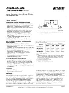
9 TheSPI Read command (slave address with R/W bit set) isthen clocked into the device. The opcode is followed byan address, with at least one data byte being clockedout of the to:00hIODIR01hIPOL02hGPINTEN03hDEFVAL04h INTCON05hIOCON06hGPPU07hINTF08hINTCAP (Read-only)09hGPIO0 AhOLAT 2004-2019 Microchip Technology 6 MCP23008/MCP23S08 FIGURE 1-1:MCP23008 I2C DEVICE Sequential Write/ReadFor sequential operations, instead of deselecting thedevice by raising CS, the master clocks the next bytepointed to by the Address sequence ends by the raising of MCP23S08 Address Pointer will roll over toaddress zero after reaching the last register Address DecoderThe hardware address pins are used to determine thedevice address. To address a device, the correspond-ing address bits in the control byte must match the pinstate. MCP23008 has address pins A2, A1 and A0. MCP23S08 has address pins A1 and pins must be biased START- RESTART- STOP- Write- Read- Device opcode- Device address- Data out from MCP23008- Data into and Sequential and Sequential ReadSWOPADDRDINPSWOPSRROPDOUTPByteSequen tialByteSequential 2004-2019 Microchip Technology 7 MCP23008 I2C DEVICES (MCP23008)The MCP23008 is a slave I2C device that supports 7-bitslave addressing, with the read/write bit filling out thecontrol byte.
10 The slave address contains four fixed bitsand three user-defined hardware address bits (pins A2,A1 and A0). Figure 1-2 shows the control byte SPI DEVICES (MCP23S08)The MCP23S08 is a slave SPI device. The slaveaddress contains five fixed bits and two user-definedhardware address bits (pins A1 and A0), with theread/write bit filling out the control byte. Figure 1-3shows the control byte 1-2:I2C CONTROL BYTE FORMATFIGURE 1-3:SPI CONTROL BYTE FORMATFIGURE 1-4:I2C ADDRESSING REGISTERSFIGURE 1-5:SPI ADDRESSING REGISTERSS0100A2 A1 A0 R/WACKS tartbitSlave AddressR/W bitACK bitControl ByteR/W = 0 = writeR/W = 1 = read01000A1 A0 R/WSlave AddressR/W bitControl ByteR/W = 0 = writeR/W = 1 = readCSS0100A2 A1 A00 ACKA7A6A5A4A3A2A1A0 ACKD evice OpcodeRegister AddressR/W = 0 The ACKs are provided by the OpcodeRegister AddressCS 2004-2019 Microchip Technology 8 MCP23008 PortThe GPIO module contains the data port (GPIO),internal pull-up resistors and the Output Latches(OLAT).