Transcription of MEMS Fabrication I : Process Flows and Bulk Micromachining
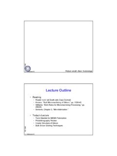
1 MEMS Fabrication I : Process Flows and Bulk Micromachining Dr. Thara Srinivasan Lecture 2. EE C245. U. Srinivasan Picture credit: Alien Technology Lecture Outline Reading Reader is in! (at South side Copy Central). Kovacs, Bulk Micromachining of Silicon, pp. 1536-43. Williams, Etch Rates for Micromachining Processing, pp. 256-60. Senturia, Chapter 3, Microfabrication.. Today's Lecture Tools Needed for MEMS Fabrication Photolithography Review Crystal Structure of Silicon Bulk Silicon Etching Techniques EE C245. U. Srinivasan . 1. IC Processing Cross-section Masks Cross-section Masks N-type Metal Oxide Semiconductor (NMOS) Process flow EE C245. Jaeger U. Srinivasan . CMOS Processing Processing steps Oxidation Photolithography Etching Chemical Vapor Jaeger Deposition Complementary Metal-Oxide-Semiconductor Diffusion Ion Implantation Evaporation and deposit Sputtering Epitaxy EE C245. etch pattern U. Srinivasan . 2. MEMS Devices Polysilicon level 1. Plate Polysilicon level 2. Polysilicon level 2 Staple Polysilicon level 1.
2 Silicon substrate EE C245. Hinge staple Silicon substrate Prof. Kris Pister Support arm U. Srinivasan . MEMS Devices Microoptomechanical switches, Lucent Caliper Thermally isolated RMS. converter Reay et al. EE C245. Analog Devices Integrated U. Srinivasan . accelerometer Microturbine, Schmidt group MIT. 3. MEMS Processing Unique to MEMS Fabrication Sacrificial etching Mechanical properties critical Thicker films and deep etching Etching into substrate Double-sided lithography 3-D assembly Wafer-bonding Molding Integration with electronics, fluidics sacrificial layer structural layer Unique to MEMS packaging and testing Delicate mechanical structures Packaging: before or after dicing? Package Sealing in gas environments EE C245. Interconnect - electrical, mechanical, fluidic Dice Testing electrical, mechanical, fluidic Release U. Srinivasan . Photolithography: Masks and Photoresist Photolithography steps Photoresist spinnning, 1-10 m spin coating Optical exposure through a photomask Developing to dissolve exposed resist Bake to drive off solvents Remove using solvents (acetone) or O2 plasma Photomasks Layout generated from CAD file Mask reticle: chrome or emulsion on fused silica 1-3 $k EE C245.
3 U. Srinivasan . light-field dark-field 4. Photoresist Application Spin-casting photoresist Polymer resin, sensitizer, carrier solvent Positive and negative photoresist Thickness depends on Concentration Viscosity Spin speed Spin time EE C245. U. Srinivasan . Photolithography Tools Contact or proximity Projection Resolution: Contact - 1-2 m, Reduce 5-10 , stepper mode Proximity - 5 m Resolution - ( /NA) ~ 1 m Depth of focus poor Depth of focus ~ Few ms Double-sided lithography EE C245. Make alignment marks on both sides of wafer Use IR imaging to see through to back side Store image of front side marks; align to back U. Srinivasan . 5. Materials for MEMS. Substrates Silicon Glass Quartz Thin Films Polysilicon Silicon Dioxide, Silicon Nitride Metals Silicon crystal structure Polymers = . EE C245. Wolf and Tauber U. Srinivasan . Silicon Crystallography [001] z z z (110). <100> y y y [010]. [100] x (100) (110) (111). x x Miller Indices (h k l). Planes Reciprocal of plane intercepts with axes Intercepts of normal to plane with plane (unique), {family}.
4 Directions EE C245. Move one endpoint to origin {111}. [unique], <family>. U. Srinivasan . 6. Silicon Crystallography 0 1/2 0. 3/4 1/4. 1/2 0 1/2. 1/4 3/4. 0 1/2 0. Angles between planes, . between [abc] and [xyz] given by: ax+by+cz = |(a,b,c)|*|(x,y,z)|*cos( ). (100),(111) = Cos 1 ((1 + 0 + 0) /(1)( 3 )). {100} and {110} 45 . EE C245. {100} and {111} . {110} and {111} , 90 and . U. Srinivasan . Silicon Crystal Origami {111} {110} {111}. (111) (101) (111). {100}. (100). [101][101]. {111} {110} {111}. (111) (101) (111). Judy {100}. (001). Silicon fold-up cube [011][011]. {110} {111} {110} {111} {110}. Adapted from Profs. Kris (011) (111) (101) (111) (011). Pister and Jack Judy [110] [110]. {110}. {110}. {110}. [001]. {110}. {100} {100} {100}. (110). (110). (110). (110). Print onto transparency [001]. (010) (100) (010). Assemble inside out [100]. {110}. [100]. {111} {110} {111} {110}. Visualize crystal plane (011) (111) (101) (111) (011). [010] [010]. orientations, intersections, EE C245.
5 {100}. and directions (001). Judy, UCLA. U. Srinivasan . 7. Silicon Wafers Location of primary and secondary flats shows Crystal orientation Doping, n- or p-type EE C245. U. Srinivasan . Maluf Mechanical Properties of Silicon Crystalline silicon is a hard and brittle material that deforms elastically until it reaches its yield strength, at which point it breaks. Tensile yield strength = 7 GPa (~1500 lb suspended from 1. mm ). Young's Modulus near that of stainless steel {100} = 130 GPa; {110} = 169 GPa; {111} = 188 GPa Mechanical properties uniform, no intrinsic stress Mechanical integrity up to 500 C. Good thermal conductor, low thermal expansion coefficient High piezoresistivity EE C245. U. Srinivasan . 8. What is Bulk EE C245. Micromachining ? U. Srinivasan . Bulk Etching of Silicon Etching modes Isotropic vs. anisotropic Reaction-limited Etch rate dependent on temperature Diffusion-limited Etch rate dependent on mixing Also dependent on layout and geometry, loading Maluf Choosing a method adsorption desorption Desired shapes surface reaction Etch depth and uniformity Surface roughness.
6 EE C245. Process compatibility Safety, cost, availability, slowest step controls environmental impact U. Srinivasan . rate of reaction 9. Wet Etch Variations, Crystalline Si Etch rate variation due to wet etch set-up Loss of reactive species through consumption Evaporation of liquids Poor mixing (etch product blocks diffusion of reactants). Contamination Applied potential Illumination Etch rate variation due to material being etched Impurities/dopants Etch rate variation due to layout Distribution of exposed area ~ loading Structure geometry EE C245. U. Srinivasan . Anisotropic Etching of Silicon Etching of Si with KOH. Si + 2OH- Si(OH)2 2+ + 4e- 4H2O + 4e- 4(OH) - + 2H2. Crystal orientation relative etch rates {110}:{100}:{111} = 600:400:1. {111} plane has three of its bonds below the surface {111} may form protective oxide quickly {111} smoother than other crystal EE C245. planes <100>. U. Srinivasan . Maluf 10. KOH Etch Conditions 1 KOH : 2 H2O (wt.), stirred bath @ 80 C. Si (100) m/min Etch masks Si3N4 0.
7 SiO2 1-10 nm/min Photoresist, Al ~ fast Micromasking by H2 bubbles leads to roughness Stirring displaces bubbles Oxidizer, surfactant additives EE C245. U. Srinivasan . Maluf Undercutting Convex corners bounded by {111} planes are attacked Maluf EE C245. Ristic U. Srinivasan . 11. Undercutting Convex corners bounded by {111} planes are attacked EE C245. U. Srinivasan . Corner Compensation Protect corners with compensation . areas in layout Mesa array for self-assembly test structures, Smith and coworkers (1995). EE C245. Hadley Alien Technology U. Srinivasan . Chang 12. Corner Compensation Self-assembly microparts, Alien Technology EE C245. U. Srinivasan . Other Anisotropic Etchants TMAH, Tetramethyl ammonium hydroxide, 10-40 (90 C). Etch rate (100) = m/min Al safe, IC compatible Etch ratio (100)/(111) = 10-35. Etch masks: SiO2 , Si3N4 ~ nm/min Boron doped etch stop, up to 40 slower EDP (115 C). Carcinogenic, corrosive Etch rate (100) = m/min Al may be etched R(100) > R(110) > R(111). Etch ratio (100)/(111) = 35.
8 Etch masks: SiO2 ~ nm/min, Si3N4 ~ nm/min EE C245. Boron doped etch stop, 50 slower U. Srinivasan . 13. Boron-Doped Etch Stop Control etch depth precisely with boron doping (p++). [B] > 1020 cm-3 reduces KOH etch rate by 20-100 . Gaseous or solid boron diffusion At high dopant level, injected electrons recombine with holes in valence band and are unavailable for reactions to give OH- Results Beams, suspended films 1-20 m layers possible p++ not compatible with CMOS. EE C245. Buried p++ compatible U. Srinivasan . Micronozzle Maluf EE C245. U. Srinivasan . 14. Microneedles Ken Wise group, University of Michigan EE C245. U. Srinivasan . Microneedles EE C245. Wise group, University of Michigan U. Srinivasan . 15. EE C245 Microneedles Wise group, University of Michigan U. Srinivasan . electrochemical Etch Stop electrochemical etch stop n-type epitaxial layer grown on p-type wafer forms p-n diode p>n electrical conduction p<n reverse bias current Passivation potential potential at which thin SiO2 layer forms, different for p- and n-Si Set-up p-n diode in reverse bias p-substrate floating etched n-layer above passivation potential not etched EE C245.
9 U. Srinivasan . Maluf 16. electrochemical Etch Stop electrochemical etching on preprocessed CMOS wafers N-type Si well with circuits suspended from SiO2 support beam Thermally and electrically isolated TMAH etchant, Al bond pads safe EE C245. Reay et al. (1994). Kovacs group, Stanford U. U. Srinivasan . Pressure Sensors Bulk micromachined pressure n-type sensors epilayer, Deposit p-type insulator Piezoresistivity change in substrate electrical resistance due to mechanical stress Diffuse In response to pressure load on piezoresistors thin Si film, piezoresistive elements change resistance Membrane deflection < 1 m Deposit &. pattern metal (100) Si Bondpad P-type diffused electrochemical Metal diaphragm piezoresistor etch of backside conductors R2 RR. n-type cavity 11 epitaxial RR3. 3 layer (111). (111). Anodic bonding EE C245. Backside Anodically port bonded of glass Etched Pyrex Maluf cavity substrate U. Srinivasan . 17. Pressure Sensors Only 150 400 900 m3. Catheter-tip pressure sensor, Lucas NovaSensor EE C245.
10 U. Srinivasan . Isotropic Etching of Silicon pure HF. reaction-limited HNA: hydrofluoric acid (HF), nitric acid (HNO3) and acetic (CH3 COOH) or water HNO3 oxidizes Si to SiO2. HF converts SiO2 to soluble H2 SiF6. Acetic prevents dissociation of HNO3. Etch masks SiO2 etched at 30-80 nm/min Nonetching Au or Si3N4. pure HNO3. EE C245. diffusion-limited Robbins U. Srinivasan . 18. Isotropic Etching Examples Tjerkstra, 1997. 5% (49%) HF : 80% (69%) HNO3 : 15% H2O (by volume). Half-circular channels for chromatography Etch rate m/min Surface roughness 3 nm Pro and Con EE C245. Easy to mold from rounded channels Etch rate and profile are highly agitation sensitive U. Srinivasan . Dry Etching of Silicon Dry etching Plasma phase sheath Vapor phase Parameters Gas and species generated ~. ions, radicals, photons RF frequency, MHz RF power, 10's to 1000's W. Pressure, mTorr >100 Torr EE C245. U. Srinivasan . e - + CF4 CF3+ + F + 2e- 19. Plasma Etching of Silicon Plasma phase etching processes (physical).